The Pulse
-
Epson Achieves 50% Energy Efficiency with QuickLogic eFPGA
2026-01-13T19:29:00+00:00
-
ESD Alliance Reports Electronic System Design Industry Posts $5.6 Billion in Revenue in Q3 2025
2026-01-13T15:37:15+00:00
-
Cadence Delivers Enterprise-Level Reliability with Next-Gen Low-Power DRAM for AI Applications Featuring Microsoft RAIDDR ECC Technology
2026-01-13T15:17:06+00:00
-
Omni Design Technologies Appoints Poh Sim Gan as Chief Financial Officer
2026-01-13T15:08:21+00:00
-
The State of HBM4 Chronicled at CES 2026
2026-01-13T10:23:52+00:00
-
Syntacore upgrades its SCR RISC-V IP: Packed-SIMD, Zicond and Zimop Extensions
2026-01-13T10:07:28+00:00
-
Industry’s First Verification IP for Arm AMBA DTI-H
2026-01-13T07:43:00+00:00
-
PermuteV: A Performant Side-channel-Resistant RISC-V Core Securing Edge AI Inference
2026-01-13T07:26:44+00:00
-
EnSilica: H1 FY 2026 Trading Update
2026-01-12T12:37:46+00:00
-
TSMC December 2025 Revenue Report
2026-01-12T06:53:11+00:00
-
ASICLAND Expands CXL Controller Development Contract with Primemas to USD 6.5 Million
2026-01-12T06:28:05+00:00
-
TES offers CAN Flexible Data-Rate Controller IP Core for System-on-Chip (SoC) Designs
2026-01-12T05:36:13+00:00
-
2025 Year in Review: Design Wins, Advanced Nodes, and Expanding Markets
2026-01-12T05:03:21+00:00
-
Impinj and EM Microelectronic Announce Gen2X Licensing Agreement
2026-01-11T20:32:11+00:00
-
LTSCT and Andes Technology Sign Strategic IP Licensing Master Agreement to accelerate RISC-V Based Advanced Semiconductor Solutions
2026-01-09T16:27:34+00:00
-
Global Semiconductor Sales Increase 29.8% Year-to-Year in November
2026-01-09T06:37:49+00:00
-
BAE Systems Licenses Time Sensitive Networking (TSN) Ethernet IP Cores from CAST
2026-01-08T17:40:00+00:00
-
HBM4 Mass Production Delayed to End of 1Q26 By Spec Upgrades and Nvidia Strategy Adjustments
2026-01-08T12:39:00+00:00
-
JESD204 Frame Mapping explained from converter samples to lanes
2026-01-08T12:32:00+00:00
-
ASICLAND Secures USD 17.6 Million Storage Controller Mass Production Contract
2026-01-08T12:21:02+00:00
-
TSMC to Lead Rivals at 2-nm Node, Analysts Say
2026-01-07T14:36:38+00:00
-
Energy-efficient RF power modules developed using SOI technology
2026-01-07T12:56:46+00:00
-
Making Strong Error-Correcting Codes Work Effectively for HBM in AI Inference
2026-01-07T09:19:56+00:00
-
Arm in the agentic era: Scaling the converged AI data center
2026-01-07T08:49:31+00:00
-
Quintauris Demonstrates RISC-V Innovation in Automotive at CES
2026-01-07T06:57:22+00:00
The Semiconductor IP Marketplace that puts you first
Semi IP Hub's mission is to provide you with a platform where you can find Silicon IP cores for your next project without being harassed by dozens of sellers.
Here, your contact details are not shared with third parties unless you request to be contacted by a supplier.
Spotlight
-
HBM4 PHY IP
- Supports JEDEC HBM4 DRAMs
- Supports data rates up to 12 Gbps
- Supports up to 32 independent 64-bit memory channels
- Pseudo-channel operation supported to enable up to 64 32-bit pseudo-channels with 2048-bit PHY
-
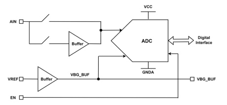
10-bit SAR ADC - XFAB XT018
- The TS_ADC_10b_X8 is a 10-bit capacitive successive approximation register (SAR) Analog-to-Digital converter (ADC).
- It operates with a 3.3 V analog power supply, a 1.8 V digital power supply, and an external voltage reference.
- The ADC converts single-ended input voltages and requires no external S/H circuit.
-
eFuse Controller IP
- AMBA 3.0 APB interface for register access
- Automated eFuse read, program, and reload operations
- Protection against repeated programming of the same bits
- Support for 32-bit aligned read/program operations
-
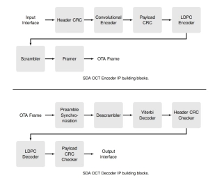
SDA OCT Encoder and Decoder
- The SDA OCT Encoder handles the construction of Over-The-Air (OTA) frames as indicated in the standard, a preamble followed by a header and payload data, with both fields being protected by cyclic redundancy check (CRC) and forward error correction (FEC).
- The SDA OCT Decoder performs the synchronization of the Over-The-Air (OTA) frame and then decodes the header and payload data within the frame.
-
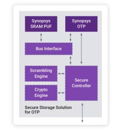
Secure Storage Solution for OTP IP
- Advanced Security: Encrypted storage in OTP using dynamic root key from SRAM PUF
- System-Level Security Extension: Add-on allows sharing the SRAM PUF to protect chip-level assets
- Flexible Security Configuration: Secure regions within OTP can be tailored to meet specific needs
-
UDP Offload Engine for IPv6
- Full IPv6 support including Echo, NDP, MLD
- Line-rate UDP/IPv6 transmit and receive
- RFC 768 & RFC 8200 compliant
- Packet parsing and header synthesis in hardware
UCIe Controller IP View All
-
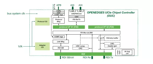
UCIe Die-to-Die Chiplet Controller
- High configurability and customizability
- Defines packets to communicate with a link partner using different AXI parameters
- Supports raw streaming modes
- Provides various Flit formats in UCIe v1.1 (filt format 2: 68B flit format, flit format 3/4: standard 256B flit format, and flit format 5/6: latency optimized 256B flit format)
-
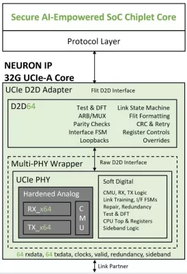
UCIe PHY & D2D Adapter
- 32Gbps UCIe-Advanced (UCIe-A) & Standard (UCIe-S)
- UCIe v1.1 specification
-
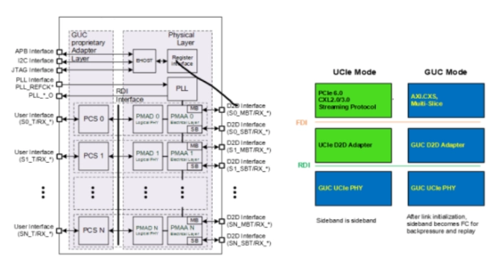
TSMC CLN5FF GUCIe LP Die-to-Die PHY
- IGAD2DY11A is an LP (Low Power) Die-to-Die (D2D) PHY for SoIC-X Face-to-Face advanced package.
- This GUCIe PHY not only supports UCIe specification rev 1.1 compliance physical layer and Raw D2D interface (RDI) but also optionally provides the
PCIe 7.0 IP View All
-
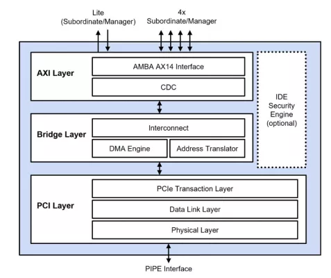
PCIe 7.0 Controller with AXI
- Optimized for high-bandwidth efficiency at data rates up to 128 GT/s
- Separate native TX/RX data path separating posted/Non posted/completion traffic
- Handles up to 4 TLPs per cycle
- Advanced PIPE modes and port bifurcation
-
PCIe 7.0 PHY IP
- Physical Coding Sublayer (PCS) block with PIPE interface
- Supports PCIe 7.0, encoding, backchannel initialization
- Lane margining at the receiver
-
PCIe 7.0 PHY in TSMC (N5, N3P)
- Physical Coding Sublayer (PCS) block with PIPE interface
- Supports PCIe 7.0, encoding, backchannel initialization
- Lane margining at the receiver
- Spread-spectrum clocking (SSC)
AI IP View All
-
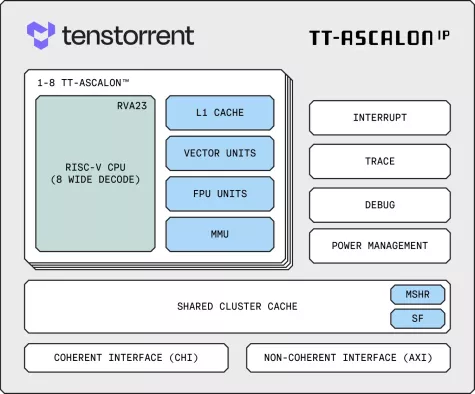
RISC-V CPU IP
- RISC-V RVA23 Compliant
- >18 SPECint2006/GHz
- 8-wide decode unit
- Advanced branch predictor
-
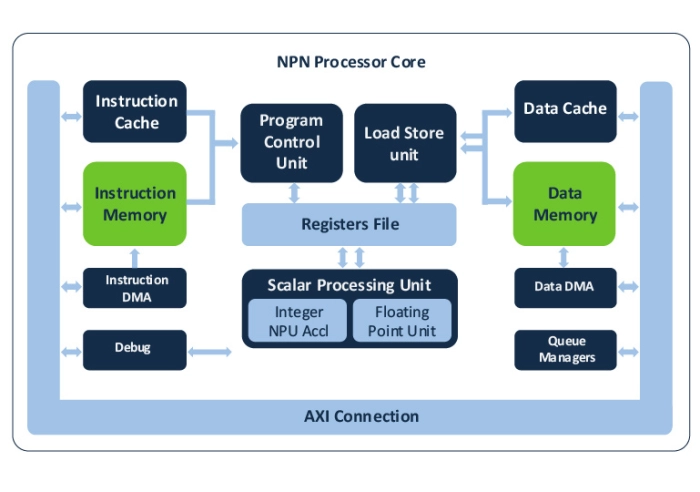
NPU IP for Embedded ML
- Fully programmable to efficiently execute Neural Networks, feature extraction, signal processing, audio and control code
- Scalable performance by design to meet wide range of use cases with MAC configurations with up to 64 int8 (native 128 of 4x8) MACs per cycle
- Future proof architecture that supports the most advanced ML data types and operators
-
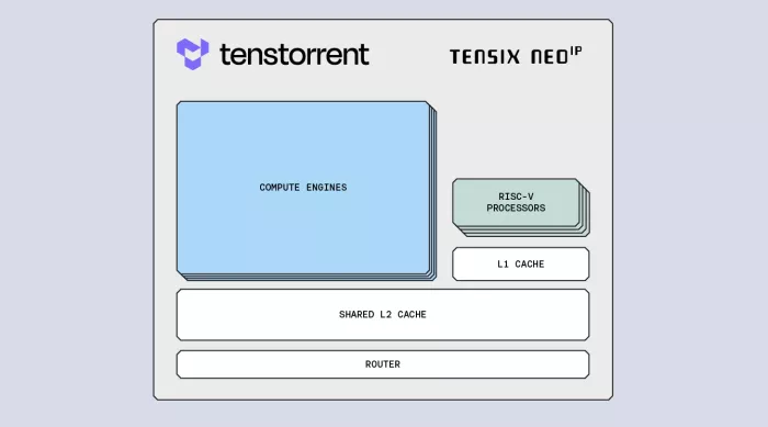
Future-proof IP for training and inference with leading performance per watt and per dollar
- RISC-V-based AI IP development for enhanced training and inference.
- Silicon-proven solutions tailored for AI workload optimization.
- Energy-efficient performance with industry-leading Perf/W.
MIPI IP View All
-
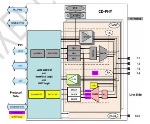
MIPI C-PHY/D-PHY Combo CSI-2 RX+ IP (6.0Gsps/trio, 4.5Gbps/lane) in TSMC N6
- Dual mode PHY Supports MIPI Alliance Specification D-PHY v2.5 & C-PHY v2.0
- Consists of 1 Clock lane and 4 Data lanes in D-PHY mode
-
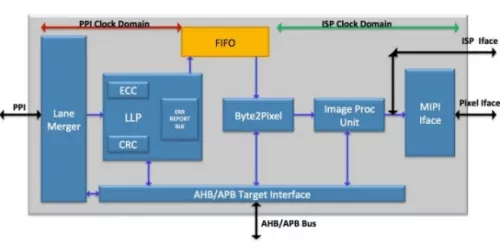
MIPI CSI-2 controller Receiver v 2.1, Compatible with MIPI C-PHY v1.2 & DPHY v2.1.
- Fully compliant to MIPI standard
- Small footprint
- Code validated with Spyglass
-
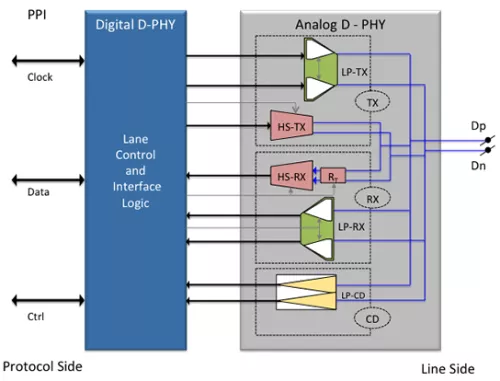
MIPI D-PHY IP for TSMC (5nm, 6/7nm, 12/16nm, 22nm, 28nm, 40nm)
- Compliant to MIPI Alliance Standard for D-PHY specification Version 2.1, 1.2, 1.1
- Supports standard PHY transceiver compliant to MIPI Specification
- Supports standard PPI interface compliant to MIPI Specification
- Supports synchronous transfer at high speed mode with a bit rate of 80-2500 Mb/s
RISC-V IP View All
-
32b/64b RISC-V 5-stage, scalar, in-order, Application Processor. Linux and multi-core capable. Maps upto ARM A-35. Optimal PPA.
- 32/64 Bit RISC-V core
- 5-stage pipeline
- In-order, Single issue
- Multicore Capable (up to 8 cores)

-
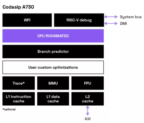
Dual-issue Linux-capable RISC-V core
- 64-bit RISC-V core
- RVA22 profile
- Linux capable
-
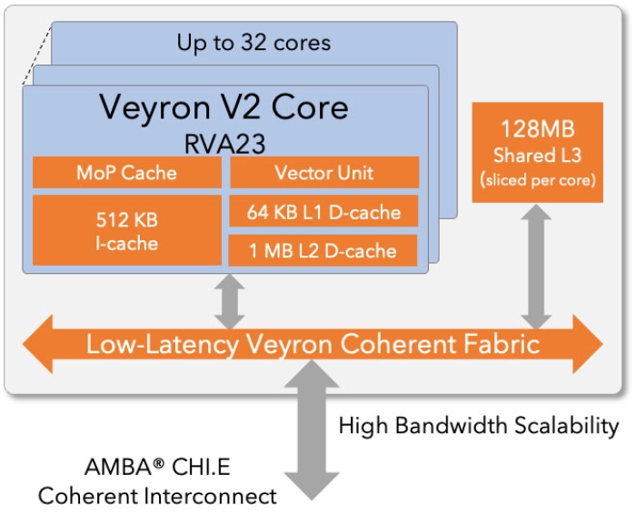
High-performance RISC-V CPU
- Fully compliant with the RVA23 RISC-V specification
- Comparable PPA to Arm Neoverse V3 / Cortex-X4
- Standard AMBA CHI.E coherent interface for SoC and chiplet integration
- Co-architected with Veyron E2 for seamless vector, AI acceleration, and big-little style heterogeneous compute configurations
