LPDDR IP
All offers in
LPDDR IP
Filter
Compare
196
LPDDR IP
from
25
vendors
(1
-
10)
-
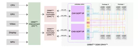
LPDDR5X/5/4X/4 combo PHY at 7nm
- Compliant with JEDEC JESD209-5B for LPDDR5X/5/4X/4 with PHY standards
- Delivering up to 8533Mbps
- DFI 5.1 specification PHY Interface Compliant
- Support up to 4 ranks

-
LPDDR5X/5/4X/4 combo PHY at Samsung SF5A
- Compliant for JEDEC standards for LPDDR5X/5/4X/4 with PHY standards
- DFI 5.1 specification PHY Interface Compliant
- Support up to 4 ranks
- x16 and x32 channel support

-
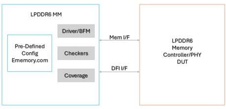
Simulation VIP for LPDDR6
- This Verification IP (VIP) is intended for modeling the upcoming JEDEC Low-Power Memory Device, LPDDR6 design specification.
- It provides a mature, highly capable compliance verification solution that supports simulation, formal analysis, and hardware acceleration platforms, making it applicable to intellectual property (IP), system-on-chip (SoC), and system-level verification.

-
LPDDR6/5X/5 PHY V2 - Intel 18A-P
- The LPDDR6/5X/5 PHY IP enables ASICs, ASSPs, system-on-chips (SoCs), and system-in-package applications requiring high-performance LPDDR6, LPDDR5X, and/or LPDDR5 SDRAM interfaces operating at up to 14.4 Gbps
- With flexible configuration options, the LPDDR6/5X/5 PHY IP can be used in a variety of applications supporting LPDDR6, LPDDR5X, and/or LPDDR5 SDRAMs, precisely targeting the specific power, performance, and area (PPA) requirements of these systems
-
LPDDR6/5X/5 PHY V2 - TSMC N6
- The LPDDR6/5X/5 PHY IP enables ASICs, ASSPs, system-on-chips (SoCs), and system-in-package applications requiring high-performance LPDDR6, LPDDR5X, and/or LPDDR5 SDRAM interfaces operating at up to 14.4 Gbps
- With flexible configuration options, the LPDDR6/5X/5 PHY IP can be used in a variety of applications supporting LPDDR6, LPDDR5X, and/or LPDDR5 SDRAMs, precisely targeting the specific power, performance, and area (PPA) requirements of these systems
- LPDDR6 SDRAM’s combination of high bandwidth, capacity, low power, and cost effectiveness makes LPDDR6/5X/5 SDRAMs an attractive solution for traditional and new markets
- The LPDDR6/5X/5 PHY IP is designed to appeal to a variety of applications including: * Traditional mobile environments * Consumer products * Automotive solutions * Artificial intelligence * Data center applications
-
LPDDR6/5X/5 PHY V2 - TSMC N5A for Automotive, ASIL B Random, AEC-Q100 Grade 2
- The LPDDR6/5X/5 PHY IP enables ASICs, ASSPs, system-on-chips (SoCs), and system-in-package applications requiring high-performance LPDDR6, LPDDR5X, and/or LPDDR5 SDRAM interfaces operating at up to 14.4 Gbps
- With flexible configuration options, the LPDDR6/5X/5 PHY IP can be used in a variety of applications supporting LPDDR6, LPDDR5X, and/or LPDDR5 SDRAMs, precisely targeting the specific power, performance, and area (PPA) requirements of these systems
- LPDDR6 SDRAM’s combination of high bandwidth, capacity, low power, and cost effectiveness makes LPDDR6/5X/5 SDRAMs an attractive solution for traditional and new markets
- The LPDDR6/5X/5 PHY IP is designed to appeal to a variety of applications including: * Traditional mobile environments * Consumer products * Automotive solutions * Artificial intelligence * Data center applications
-
LPDDR6/5X/5 PHY V2 - TSMC N4P
- The LPDDR6/5X/5 PHY IP enables ASICs, ASSPs, system-on-chips (SoCs), and system-in-package applications requiring high-performance LPDDR6, LPDDR5X, and/or LPDDR5 SDRAM interfaces operating at up to 14.4 Gbps
- With flexible configuration options, the LPDDR6/5X/5 PHY IP can be used in a variety of applications supporting LPDDR6, LPDDR5X, and/or LPDDR5 SDRAMs, precisely targeting the specific power, performance, and area (PPA) requirements of these systems
- LPDDR6 SDRAM’s combination of high bandwidth, capacity, low power, and cost effectiveness makes LPDDR6/5X/5 SDRAMs an attractive solution for traditional and new markets
- The LPDDR6/5X/5 PHY IP is designed to appeal to a variety of applications including: * Traditional mobile environments * Consumer products * Automotive solutions * Artificial intelligence * Data center applications
-
LPDDR6/5X/5 PHY V2 - TSMC N4C
- The LPDDR6/5X/5 PHY IP enables ASICs, ASSPs, system-on-chips (SoCs), and system-in-package applications requiring high-performance LPDDR6, LPDDR5X, and/or LPDDR5 SDRAM interfaces operating at up to 14.4 Gbps
- With flexible configuration options, the LPDDR6/5X/5 PHY IP can be used in a variety of applications supporting LPDDR6, LPDDR5X, and/or LPDDR5 SDRAMs, precisely targeting the specific power, performance, and area (PPA) requirements of these systems
- LPDDR6 SDRAM’s combination of high bandwidth, capacity, low power, and cost effectiveness makes LPDDR6/5X/5 SDRAMs an attractive solution for traditional and new markets
- The LPDDR6/5X/5 PHY IP is designed to appeal to a variety of applications including: * Traditional mobile environments * Consumer products * Automotive solutions * Artificial intelligence * Data center applications
-
LPDDR6/5X/5 PHY V2 - TSMC N3P
- The LPDDR6/5X/5 PHY IP enables ASICs, ASSPs, system-on-chips (SoCs), and system-in-package applications requiring high-performance LPDDR6, LPDDR5X, and/or LPDDR5 SDRAM interfaces operating at up to 14.4 Gbps
- With flexible configuration options, the LPDDR6/5X/5 PHY IP can be used in a variety of applications supporting LPDDR6, LPDDR5X, and/or LPDDR5 SDRAMs, precisely targeting the specific power, performance, and area (PPA) requirements of these systems
- LPDDR6 SDRAM’s combination of high bandwidth, capacity, low power, and cost effectiveness makes LPDDR6/5X/5 SDRAMs an attractive solution for traditional and new markets
- The LPDDR6/5X/5 PHY IP is designed to appeal to a variety of applications including: * Traditional mobile environments * Consumer products * Automotive solutions * Artificial intelligence * Data center applications
-
LPDDR6/5X/5 PHY - TSMC N3P
- The LPDDR6/5X/5 PHY IP enables ASICs, ASSPs, system-on-chips (SoCs), and system-in-package applications requiring high-performance LPDDR6, LPDDR5X, and/or LPDDR5 SDRAM interfaces operating at up to 14.4 Gbps
- With flexible configuration options, the LPDDR6/5X/5 PHY IP can be used in a variety of applications supporting LPDDR6, LPDDR5X, and/or LPDDR5 SDRAMs, precisely targeting the specific power, performance, and area (PPA) requirements of these systems
- LPDDR6 SDRAM’s combination of high bandwidth, capacity, low power, and cost effectiveness makes LPDDR6/5X/5 SDRAMs an attractive solution for traditional and new markets
- The LPDDR6/5X/5 PHY IP is designed to appeal to a variety of applications including: * Traditional mobile environments * Consumer products * Automotive solutions * Artificial intelligence * Data center applications