The Pulse
-
瑞萨电子下一代 R-Car 汽车技术采用 Arteris 片上网络 IP
2026-03-25T06:42:23+00:00
-
智原主打40纳米SONOS eNVM 提供MCU设计NOR Flash替代方案
2026-03-24T06:47:47+00:00
-
香港RISC-V联盟正式成立,产学研投跨界协同 | 赋能开源芯片生态,建立国际交流门户与场景应用枢纽
2026-03-23T07:14:00+00:00
-
M31 2025年营收达17.8亿元创新高 先进制程权利金贡献浮现
2026-03-13T12:28:04+00:00
-
Innatera采用新思科技仿真解决方案 扩展面向边缘设备的类脑处理器
2026-03-12T12:24:02+00:00
-
Rambus推出業界領先HBM4E控制器IP,為AI記憶體效能樹立新標竿
2026-03-12T06:36:16+00:00
-
ZeroRISC與頂尖研究機構共同推出針對開放原始碼晶片的生產級後量子密碼技術
2026-03-11T04:54:31+00:00
-
六角形半导体的天相芯HX77采用芯原Nano IP组合,打造超低能耗AR显示处理器
2026-03-10T06:25:18+00:00
-
Allegro DVT 发布 DWP300 DeWarp 半导体 IP
2026-03-09T12:54:25+00:00
-
Cadence 推出 ChipStack™ AI Super Agent,开辟芯片设计与验证新纪元
2026-03-05T12:23:00+00:00
-
Arteris 片上网络技术在全球范围内实现了 40 亿颗芯片和芯粒的部署里程碑
2026-03-04T07:00:41+00:00
-
智原扩大UMC 14纳米工艺IP布局 锁定边缘AI与消费级市场
2026-03-03T07:01:20+00:00
-
GUC UCIe 64G IP在台积电N3P上完成流片
2026-02-25T18:14:00+00:00
-
MIPI Alliance发布UniPro v3.0与M-PHY v6.0,加速移动、PC及车载领域边缘人工智能的JEDEC UFS性能提升
2026-02-24T14:31:50+00:00
-
proteanTecs 与孤波科技强强联手,为先进半导体系统提供统一分析解决方案
2026-02-24T06:29:51+00:00
-
M31完成4纳米 MIPI M-PHY v5.0硅验证,加速布局 UFS 4.1 高速存储与车载市场
2026-02-23T07:03:23+00:00
-
ChipAgents完成7,400万美元融资,加速拓展Agentic AI平台,推动芯片设计创新提速
2026-02-19T06:22:15+00:00
-
恩智浦扩大Arteris技术部署以加速边缘AI领域领导地位
2026-02-12T05:57:58+00:00
-
SmartDV与Mirabilis Design宣布就SmartDV IP系统级模型达成战略合作
2026-02-11T08:33:01+00:00
-
Imagination Technologies 任命 Markus Mosen 为首席执行官
2026-02-10T12:40:15+00:00
-
全球首款120通道PCIe5交换芯片面世,为国产AI基础设施赋能
2026-02-06T12:54:19+00:00
-
晶心科技發布 RISC-V Now! by Andes — 聚焦商用與量產級之RISC-V 全球研討會
2026-02-06T06:58:50+00:00
-
芯原增强版ISP8200-FS系列IP获ASIL B功能安全认证
2026-02-05T06:39:25+00:00
-
Telechips与DivX续签集成电路技术许可协议
2026-01-28T15:27:55+00:00
-
Lightmatter 与创意电子 (GUC) 携手合作为 AI 云端大厂提供共同封装光学 (CPO) 解决方案
2026-01-28T06:48:00+00:00
The Semiconductor IP Marketplace that puts you first
Semi IP Hub's mission is to provide you with a platform where you can find Silicon IP cores for your next project without being harassed by dozens of sellers.
Here, your contact details are not shared with third parties unless you request to be contacted by a supplier.
Spotlight
-
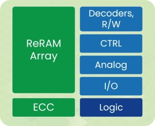
ReRAM NVM in DB HiTek 130nm BCD
- 10K cycles endurance
- >10 years retention at 125°C
- Ultra-low power consumption
- Low-cost NVM – requires only two additional masks
-
Crystal Oscillator for a 32 kHz Crystal - GLOBALFOUNDRIES® 22FDX®
- Specific crystal: 32 kHz
- Supported series resistance: up to 100 kOhm
- Supported load capacitance: 3 pF to 12.5 pF
- Startup time: 59 ms (TT, 12 pF) depending on crystal and PCB
-
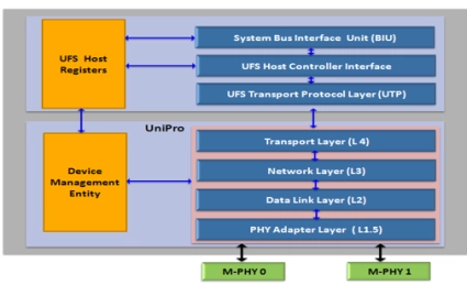
UFS 5.0 Host Controller IP
- UFS 5.0
- UFS HCI 5.0
- MIPI UniPro version 3.0
- MIPI M-PHY version 6.0
-
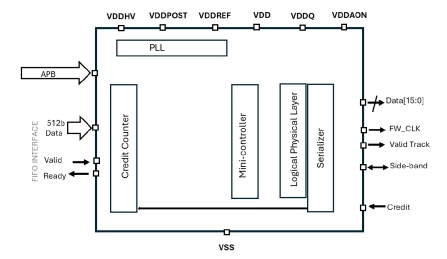
UCIe TX Interface
- Transmit-only UCIe REV1.1 with FIFO Interface
- TSMC 16FFC process
- Low power UCIe D2D
- 1 pJ/bit at 0.7V
-
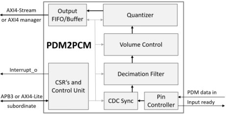
PDM Receiver/PDM-to-PCM Converter
- This PDM2PCM is a configurable audio interface core that converts a mono or stereo Pulse Density Modulation (PDM) stream into standard Pulse Code Modulation (PCM) format.
- PCM output widths are programmable from 2 to 32 bits, and all standard audio sampling rates are achievable via an adjustable Oversampling Ratio (OSR) from 32x to 256x.
-
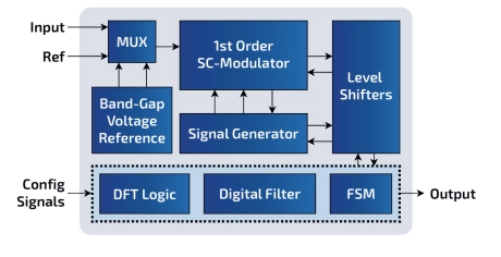
Voltage and Temperature Sensor with integrated ADC - GlobalFoundries® 22FDX®
- Voltage and temperature monitoring
- 3 single-ended voltage measurement inputs
- Operating temperature range: -40°C to 150°C
- Temperature measurement with accuracy up to 1°K ± 1°K change in temperature
UCIe Controller IP View All
-
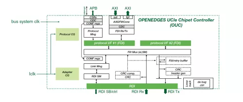
UCIe Die-to-Die Chiplet Controller
- High configurability and customizability
- Defines packets to communicate with a link partner using different AXI parameters
- Supports raw streaming modes
- Provides various Flit formats in UCIe v1.1 (filt format 2: 68B flit format, flit format 3/4: standard 256B flit format, and flit format 5/6: latency optimized 256B flit format)
-
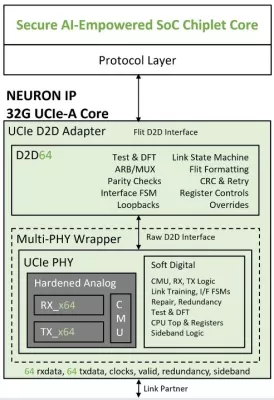
UCIe PHY & D2D Adapter
- 32Gbps UCIe-Advanced (UCIe-A) & Standard (UCIe-S)
- UCIe v1.1 specification
-
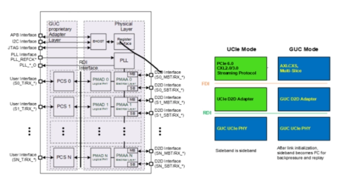
TSMC CLN5FF GUCIe LP Die-to-Die PHY
- IGAD2DY11A is an LP (Low Power) Die-to-Die (D2D) PHY for SoIC-X Face-to-Face advanced package.
- This GUCIe PHY not only supports UCIe specification rev 1.1 compliance physical layer and Raw D2D interface (RDI) but also optionally provides the
PCIe 7.0 IP View All
-
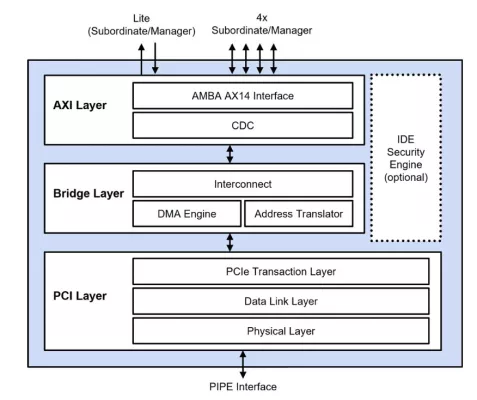
PCIe 7.0 Controller with AXI
- Optimized for high-bandwidth efficiency at data rates up to 128 GT/s
- Separate native TX/RX data path separating posted/Non posted/completion traffic
- Handles up to 4 TLPs per cycle
- Advanced PIPE modes and port bifurcation
-
PCIe 7.0 PHY IP
- Physical Coding Sublayer (PCS) block with PIPE interface
- Supports PCIe 7.0, encoding, backchannel initialization
- Lane margining at the receiver
-
PCIe 7.0 PHY in TSMC (N5, N3P)
- Physical Coding Sublayer (PCS) block with PIPE interface
- Supports PCIe 7.0, encoding, backchannel initialization
- Lane margining at the receiver
- Spread-spectrum clocking (SSC)
AI IP View All
-
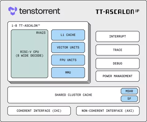
RISC-V CPU IP
- RISC-V RVA23 Compliant
- >18 SPECint2006/GHz
- 8-wide decode unit
- Advanced branch predictor
-
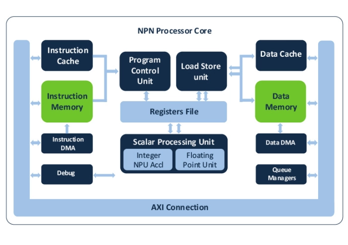
NPU IP for Embedded ML
- Fully programmable to efficiently execute Neural Networks, feature extraction, signal processing, audio and control code
- Scalable performance by design to meet wide range of use cases with MAC configurations with up to 64 int8 (native 128 of 4x8) MACs per cycle
- Future proof architecture that supports the most advanced ML data types and operators
-
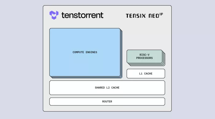
Future-proof IP for training and inference with leading performance per watt and per dollar
- RISC-V-based AI IP development for enhanced training and inference.
- Silicon-proven solutions tailored for AI workload optimization.
- Energy-efficient performance with industry-leading Perf/W.
MIPI IP View All
-
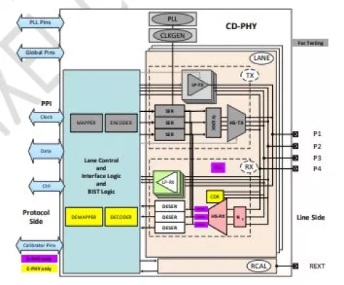
MIPI C-PHY/D-PHY Combo CSI-2 RX+ IP (6.0Gsps/trio, 4.5Gbps/lane) in TSMC N6
- Dual mode PHY Supports MIPI Alliance Specification D-PHY v2.5 & C-PHY v2.0
- Consists of 1 Clock lane and 4 Data lanes in D-PHY mode
-
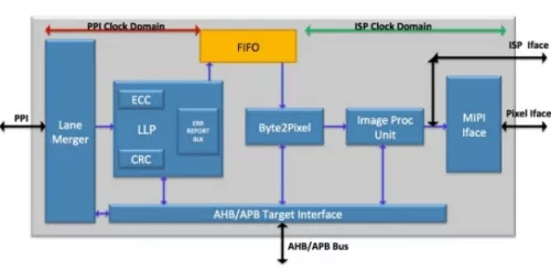
MIPI CSI-2 controller Receiver v 2.1, Compatible with MIPI C-PHY v1.2 & DPHY v2.1.
- Fully compliant to MIPI standard
- Small footprint
- Code validated with Spyglass
-
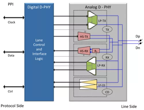
MIPI D-PHY IP for TSMC (5nm, 6/7nm, 12/16nm, 22nm, 28nm, 40nm)
- Compliant to MIPI Alliance Standard for D-PHY specification Version 2.1, 1.2, 1.1
- Supports standard PHY transceiver compliant to MIPI Specification
- Supports standard PPI interface compliant to MIPI Specification
- Supports synchronous transfer at high speed mode with a bit rate of 80-2500 Mb/s
RISC-V IP View All
-
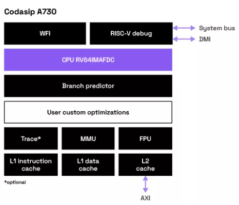
32b/64b RISC-V 5-stage, scalar, in-order, Application Processor. Linux and multi-core capable. Maps upto ARM A-35. Optimal PPA.
- 32/64 Bit RISC-V core
- 5-stage pipeline
- In-order, Single issue
- Multicore Capable (up to 8 cores)

-
Dual-issue Linux-capable RISC-V core
- 64-bit RISC-V core
- RVA22 profile
- Linux capable
-
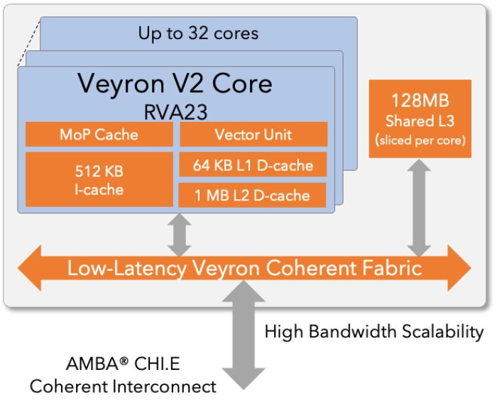
High-performance RISC-V CPU
- Fully compliant with the RVA23 RISC-V specification
- Comparable PPA to Arm Neoverse V3 / Cortex-X4
- Standard AMBA CHI.E coherent interface for SoC and chiplet integration
- Co-architected with Veyron E2 for seamless vector, AI acceleration, and big-little style heterogeneous compute configurations
