Peripheral IP
Welcome to the ultimate Peripheral IP hub! Explore our vast directory of Peripheral IP
All offers in
Peripheral IP
Filter
Compare
916
Peripheral IP
from
83
vendors
(1
-
10)
-
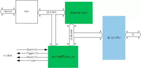
syn1588® enabled IEEE 1588 compliant clock synchronisation
- fully synchronous to the system clock
- all registers of the core operate with the rising clock edge
- well commented, structured VHDL source code
- medium footprint and medium I/O count
-
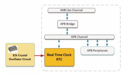
APB Real Time Clock
- The Real Time Clock (RTC) is a clock-calendar IP core that keeps track of the “Time of Day”.
- The core is organized as a series of BCD counters that counts Seconds, Minutes, Hours, Days, Months and Years (Time Units).
- The RTC seconds counter time base is generated from a clock input that is separate from the system clock.
-
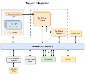
RISC-V Debug & Trace IP
- 10xEngineers Debug & N-Trace IP delivers a unified Debug + Trace solution that provides full-system visibility with low overhead and multi-hart awareness.
- Standards-compliant debug, real-time trace, and flexible triggering significantly reduce bring-up time and simplify system integration.
-
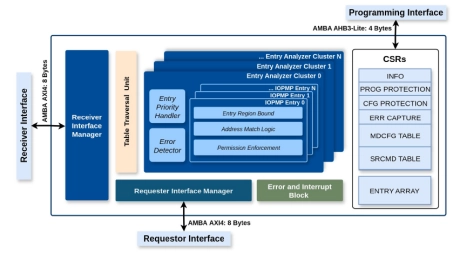
RISC-V IOPMP IP
- The I/O Physical Memory Protection (IOPMP) unit is a hardware-based access control mechanism designed to safeguard memory regions in RISC-V SoCs.
- It ensures only authorized devices and masters can access sensitive memory areas, enabling secure and reliable system operation.
-
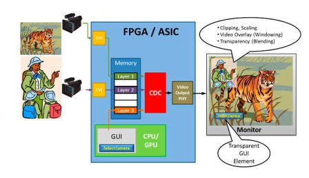
Customizable Display Controller IP
- CDC is a fully Customizable Display Controller IP supporting up to 16k resolutions (4096x4096 pixel) on a MIPI-DPI compliant parallel video output.
- Several features can be configured at synthesis time and programmed at run time.
- The display controller can be applied to e.g. FPGA systems with a resource optimized, application specific feature configuration or to ASIC projects applying a more generic feature set and thus more flexibility.
-
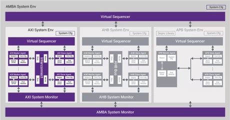
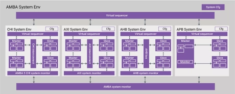
Verification IP for Arm AMBA ACE Protocol
- Complete protocol support for AMBA ACE 5, H, J and K, ACE4, ACE-Lite, AXI5, AXI4, AXI4-Lite, and AXI3.
- Configurable interconnect model for AXI5, AXI4, AXI, ACE5, and ACE4
- Backdoor access to ACE primary cache

-
Verification IP for AMBA AHB
- Complete protocol support for AHB5, AHB3, AHB2, AHB-Lite, and AHB Multi Layer
- Includes primary, secondary, monitor
- Configurable bus model
- Backdoor access to AHB secondary memory

-
Verification IP for AMBA APB
- Native SystemVerilog/Verilog with UVM
- Includes primary, secondary, monitor
- Runs natively on all major simulators
- Built-in UVM sequence library

-
Verification IP for Arm AMBA CHI Protocol
- AMBA 5 CHI-A/B/C/D/E/F/G
- Request node, secondary node agents and monitor
- Complete port-level checks
- Supports all interface types
-
Verification IP for AMBA AXI
- Complete protocol support for AXI5, AXI-J/K, AXI4, AXI4-Lite, AXI3
- Programmable number of Managers, Subordinates, and Port Monitors
- Interconnect model
- System Monitor