ADC / DAC IP
Most of the signals directly encountered in science and engineering are continuous: light intensity that changes with distance; voltage that varies over time; a chemical reaction rate that depends on temperature, etc. ADC IPs (Analog-to-Digital Converter) and DAC IPs (Digital-to-Analog Converter) are the IP cores that allow digital designs to interact with these everyday signals.
All offers in
ADC / DAC IP
Filter
Compare
744
ADC / DAC IP
from
63
vendors
(1
-
10)
-
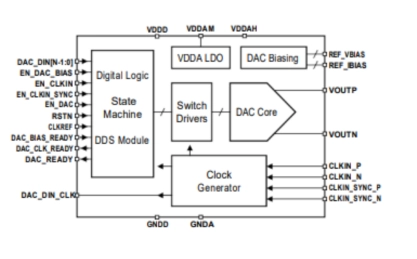
14-bit, 1200 MSPS Ultra Low Power ADC in 28nm CMOS
- 14-bit resolution, sampling rate up to 1200 MSPS
- Fully differential operation, fully specified from -40C to 125C
- Ultra low power dissipation
- Internal bandgap and voltage reference
-
Ultra high-performance low-power ADC
- TSMC 28nm
- Ultra high-performance low-power ADC
- 12-bit ADC resolution
- Sampling rate up to 5GSPS
-
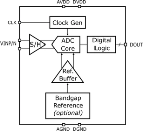
10-bit SAR ADC - XFAB XT018
- The TS_ADC_10b_X8 is a 10-bit capacitive successive approximation register (SAR) Analog-to-Digital converter (ADC).
- It operates with a 3.3 V analog power supply, a 1.8 V digital power supply, and an external voltage reference.
- The ADC converts single-ended input voltages and requires no external S/H circuit.
-
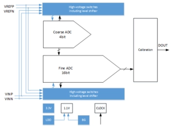
12-bit/16-bit SAR ADC
- 12 bits 100Msps SAR ADC on 28nm process;
- 12 bits 25Msps SAR ADC and Pipeline ADC above 100Msps on 40/55nm process;
- 16 bits 2/1Msps SAR ADC on 40/55nm process;
-
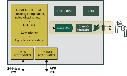
24-bit audio inductor-less class-D DAC with efficiency and ultra-low latency capability
- Provide a top-tier performances audio DAC to fabless and IC companies willing to integrate audio features directly in their product and not using external IC
- High energy efficiency, ow power consumption,
- Ultra low latency for Active Noise Cancellation
- Embedded low noise voltage regulator for best resilience to power supply noise
-
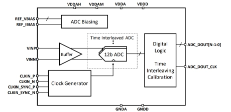
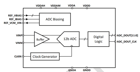
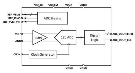
12-bit 400MSPS ADC on TSMC 7nm
- The ODT-ADS-12B2400M-7T is an ultra low power ADC designed for use in a 6/7nm CMOS process.
- This 12-bit, 400MSPS ADC supports input signals up to 200MHz and features a differential full-scale range of 1.0Vpp and excellent static and dynamic performance.
-
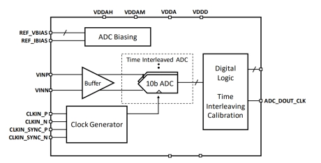
10-bit 2.5GSPS ADC
- The ODT-ADS-10B2P5G-T16 is an ultra lowpower, high-performance time-interleaved ADC designed in a 16nm CMOS process.
- This 10-bit, 2.5GSPS ADC supports input signals up to 1.0 GHz and features a differential full-scale range of 1.0Vpp with excellent static and dynamic performance.
-
12 bit, 200 MSPS ADC on TSMC 16nm FFC
- The ODT-ADS-12B200M-16FFCT is an ultra low power ADC designed in a 16nm CMOS process.
- This 12-bit, 200MSPS ADC supports input signals up to 100MHz and features a differential full-scale range of 1.0Vpp and excellent static and dynamic performance.
-
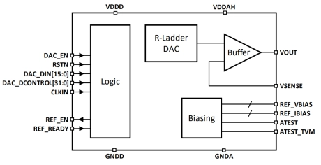
16-bit 5MSPS DAC on TSMC 16 FFC
- The ODT-DAC-16B5M-SV-T16 is an ultra-low power, voltage output, 16-bit DAC with a high performance, class AB output buffer.
- The DAC uses a proprietary architecture that guarantees monotonicity. It also features low glitch, low drift, small area and low power consumption.
- VSENSE pin is provided to set the load voltage with high accuracy. Both VOUT and VSENSE pins must be routed to the load.
-
12-bit, 2 GSPS High Performance RF DAC in 12nm CMOS
- The ODT-DAC-12B2G-12 is a high-performance current steering 12-bit DAC that operates at an update rate of up to 2GSPS.
- The DAC uses a proprietary architecture that reduces harmonic and intermodulation distortions at high output frequency and amplitudes.
- The high-performance DAC supports 20mA (maximum) differential output current and achieves up to -149dBm/Hz noise spectral density with excellent SFDR.