Other
All offers in
Other
Filter
Compare
133
Other
from
27
vendors
(1
-
10)
-
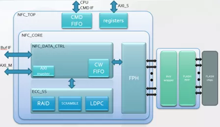
NAND Flash Controller
- The NFC IP is a NAND Flash Controller for accessing user data from NAND Flash chips.
- It is designed with scalability in mind and provides standard AXI interface for the ease of integration in SoC design.
- The NFC has many configurable features to support the requirements for different NAND Flash applications.
-
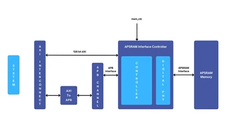
ApSRAM Controller
- The ApSRAM controller is a flexible, low-power, and low-latency solution designed for SRAM replacement in high-performance systems.
- Scalable from 64Mb to 1Gb, its multi-bank architecture enhances timing throughput, making it ideal for wearables, IoT devices, displays, automotive systems, industrial automation, and consumer electronics.
- Optimized for AI/ML, edge computing, and high-performance embedded systems, it supports seamless integration through its configurable AXI interface and adaptability across FPGA, Gate array, and Standard cell technologies.
-
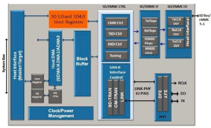
eMMC Host Controller IP
- The eMMC Host controller IP handles all of the timing and interface protocol requirements to access these media as well as processing the commands in hardware thereby scaling in both performance and access speeds.
- The eMMC 4.51 Host IP supports connection to a single slot and performs multi-block writes and erases that lower access overhead.
-
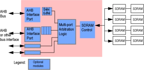
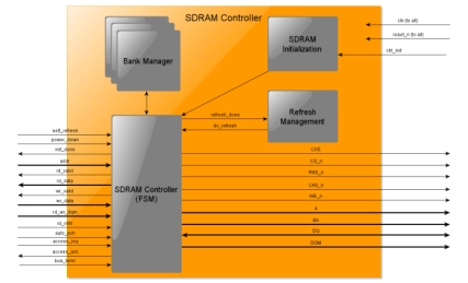
AMBA AHB Bus to SDRAM Controller
- SDRAM controller interfaces directly with AHB Bus and user interface.
- Built-in arbitration between two access ports.
- Second access port allows memory sharing with user logic devices.
- Dual write buffer for simultaneous write posting and SDRAM access.
-
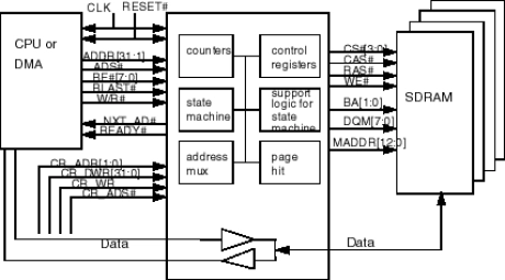
Pipeline SDRAM Controller
- Designed with synthesizable HDL for ASIC and PLD synthesis.
- Supports both discrete SDRAM chips and PC100/133 SDRAM DIMM.
- Supports register mode and non-register mode SDRAM DIMM.
- Supports industrial standard SDRAM from 64Mbit to 256Mbit device sizes.
-
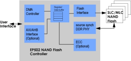
Synchronous ONFI NAND Flash Controller
- Supports single-level and multi-level cells (SLC and MLC) NAND Flash devices.
- Compatible with ONFI 2.1 Flash Interface for synchronous and asynchronous access.
- Supports source synchronous double data rate data transfer for highest possible data bandwidth.
- Supports 2k and 4k page sizes.
-
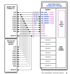
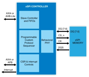
xSPI Multiple Bus Memory Controller
- SLL’s unified xSPI Multiple Bus Memory Controller IP supports the widest range of JEDEC xSPI and xSPI-like NOR Flash and PSRAM memories (JEDEC xSPI Profile 1.0 and 2.0, HyperBus 1.0, 2.0 and 3.0, OctaBus and Xccela Bus) that are available now from many memory vendors.
- JEDEC xSPI and xSPI-like memories offer good performance with lower hardware and power costs. Memory device variants offer up to 512 Mbit PSRAM, up to 2 Gigabit NOR Flash, up to 250 MHz DDR clock speeds, with x4, x8 and x16 data path widths, and a wide range of package options including 4mm x 4mm BGA49 and tiny WLCSP footprints. Some PRSAM devices are now also available with internal ECC.
-
SDRAM Controller DO-254 IP Core
- The SDRAM Controller implements a controller for Single Data Rate Synchronous Dynamic Random Access Memory (SDR SDRAM) devices as specified in the JEDEC Standard No. 21-C Page 3.11.5.1 Release 12.
- Single Data Rate SDRAM can accept one command and transfer one word of data per clock cycle.
-
xSPI NOR/NAND Flash & HyperRAM Controller
- Memory mapped access to the connected flash devices
- Continuous Burst transfer support
- Auto boot support
-
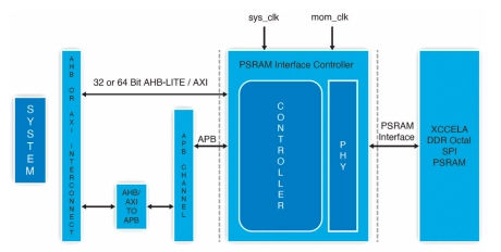
Octal SPI DDR PSRAM controller
- This controller supports AP Memory’s Xccela open standard Bus for digital interconnect and data communications, suitable for non-volatile and volatile memories such as PSRAM.
- This controller enables smooth integration AP memory’s of Xccela PSRAM memory chips into various new-gen devices made with mobile and wearable low power SoCs’.
- This memory controller implementation is designed to give the user full flexibility for driving the memory control signals and timing adjustment for data sampling.