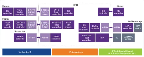
I/O Library IP
Welcome to the ultimate I/O Library IP hub! Explore our vast directory of I/O Library IP
All offers in
I/O Library IP
Filter
Compare
1,243
I/O Library IP
from
50
vendors
(1
-
10)
-
Stand-Alone ESD Cell in GF 28nm
- This ESD library is a silicon-proven set of discrete, pad-independent ESD clamps for GlobalFoundries 28nm technology.
- The library is designed to provide robust ESD protection for power domains and low-speed signals in advanced SoCs where traditional pad-based protection is insufficient or impractical.
-
I/O Library with LVDS in SkyWater 90nm
- A SkyWater I/O Library combining standard GPIO, I2C-compatible ODIO, analog I/O, and integrated LVDS for robust mixed-signal and moderate-speed differ ential interfaces.
-
General Purpose I/O
- Silvaco develops General Purpose I/O optimized for design flexibility, performance and ESD protection. We also provide specialty I/O, such as high speed LVDS (2Gbs) and SSTL, plus I/O for cryogenic applications.
-
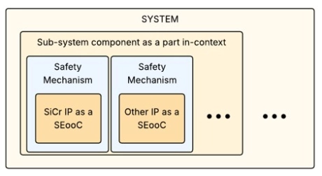
Automotive Grade PLLs, Oscillators, SerDes PMAs, LVDS/CML IP
- TSMC IP9000 Alliance member enabling automotive IP support in TSMC automotive processes
- Automotive Documentation including Safety Manual, FMEDA and DFMEA
- Design reliability report containing EM/IR and Aging analysis
-
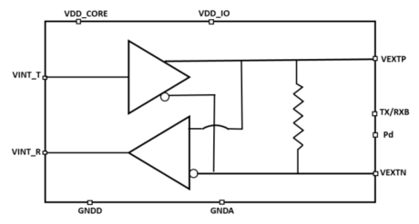
1 Gb/s LVDS Bidirectional IO on 12nm
- The ODT-LVDS-BID1G-12nm is a high-speed Bidirectional LVDS IO cell capable of operating up to 1 Gb/s.
- The ODT-LVDS-BID1G-12nm uses a high-speed signal path that can provide low jitter for input ranges of up to 1 Gb/s input.
- It also features small area and low power consumption.
- It includes the internal termination resistor and ESD protection diodes on the VEXTP and VEXTN pins.
-
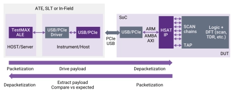
SLM High-Speed Access & Test IP
- The SLM High-Speed Access and Test (HSAT) IP combined with the TestMAX® ALE software uses standard high speed IO interfaces such as PCIe and USB, to get test, debug and monitoring data in and out of an SoC at Gigabit data rates and avoids the need for large numbers of test and interface pins.
- Test time can be reduced because the link between the test time and GPIO data rate is eliminated. Further, this solution provides a key component for Synopsys Silicon Lifecycle Management solution allowing manufacturing tests to be repeated in-system and in-field as well as providing high speed access to PVT and functional monitor dat
-
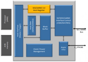
SD 3.0 / SDIO 3.0 / eMMC 5.1 Host Controller IP
- The SD 3.0 / eMMC 5.1 Host IP handles all of the timing and interface protocol requirements to access these media as well as processing the commands in hardware thereby scaling in both performance and access speeds.
- The IP supports connection to a single slot and performs multi-block writes and erases that lower access overhead.
-
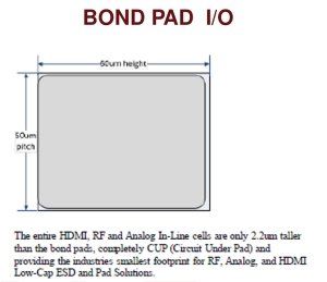
HDMI, LVDS, RF and Analog Pads in TSMC 45/40nm
- A 1.0V to 5V Analog I/O library that includes an HDMI, LVDS, and Analog/RF Low Capacitance pad set in TSMC 45/40nm HPM process.
- This library is collection of analog only IO and Power/Ground pads that include ESD. The target applications are high performance analog interfaces including HDMI, RF, LVDS, basic analog and other applications.
- The pads include a host of specialty features including fail safe, low capacitance, high ESD protection, and IEC robustness.
-
Samsung 8LPU 3.3V SD/eMMC PHY
- Synopsys SD/eMMC PHY provides an optimal balance for cost and performance for storage solutions
- Synopsys SD/eMMC PHY is a hard IP that can be used to implement a single interface that can accomplish 4-bit, 8-bit eMMC & 4-bit SD operations
- It includes an optional digi logic circuitry which is required for high-speed operations
- It complies with eMMC 5.1 (JESD84-B51A) and SDIO 6.0 JEDEC standards

-
GF 22FDX 1.8V/3.3V SD/eMMC PHY AG2 Platform
- Synopsys SD/eMMC PHY provides an optimal balance for cost and performance for storage solutions
- Synopsys SD/eMMC PHY is a hard IP that can be used to implement a single interface that can accomplish 4-bit, 8-bit eMMC & 4-bit SD operations
- It includes an optional digi logic circuitry which is required for high-speed operations
- It complies with eMMC 5.1 (JESD84-B51A) and SDIO 6.0 JEDEC standards