Analog IP
Analog IP generally handles every feature on a chip that connects to the outside world, plus power management and clocking.
Analog IP cores in this category include PLLs that generate various clocks, A/D converter IP and D/A converter IP that convert analog and digital signals, sensor IPs that measure temperature and voltage, and analog functional parts for configuring analog front ends (AFEs).
Explore our vast directory of Analog IP cores below.
All offers in
Analog IP
Filter
Compare
5,724
Analog IP
from
112
vendors
(1
-
10)
-
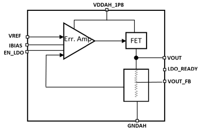
Low Dropout (LDO) Regulator
- Input voltage of 1.8V
- Output voltage of 1.35V
- Up to 100mA output current.
- Stable with Off-chip capacitor 1uF
-
-
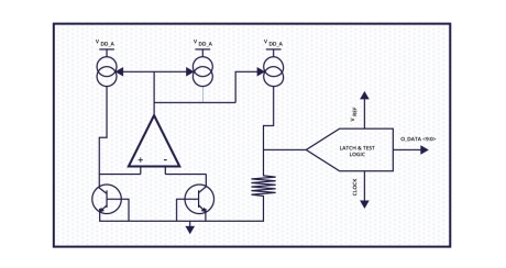
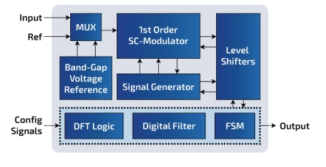
Voltage and Temperature Sensor with integrated ADC - GlobalFoundries® 22FDX®
- Voltage and temperature monitoring
- 3 single-ended voltage measurement inputs
- Operating temperature range: -40°C to 150°C
- Temperature measurement with accuracy up to 1°K ± 1°K change in temperature
-
Crystal Oscillator for a 32 kHz Crystal - GLOBALFOUNDRIES® 22FDX®
- Specific crystal: 32 kHz
- Supported series resistance: up to 100 kOhm
- Supported load capacitance: 3 pF to 12.5 pF
- Startup time: 59 ms (TT, 12 pF) depending on crystal and PCB

-
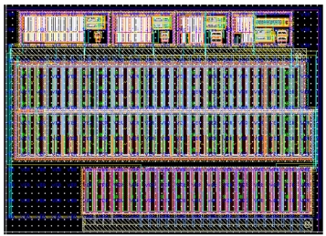
Clock Buffer - X-FAB XT018-0.18µm BCD-on-SOI CMOS
- Max Load: 25pF total (including padcell and bondwire parasitics)
- Signal Integrity: Maintains tight rise/fall timing (1.4-3.1ns) across a wide load range (1pF to 26pF)
- Low Propagation Delay: 6ns typical delay at max load, ensuring fast response for real-time systems
- Efficient Power Use: 6.5mA average current at 40MHz with 25pF load, balancing performance and energy efficiency
-
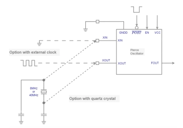
8MHz / 40MHz Pierce Oscillator - X-FAB XT018-0.18µm
- The TS_XOSC_40M_X8 is a 8MHz / 40MHz Pierce oscillator that generates a VCC-level logic square wave when a 8MHz / 40MHz quartz crystal is connected between its output XOUT and input XIN with external grounded load capacitors.
-
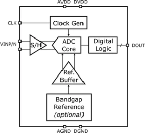
14-bit, 1200 MSPS Ultra Low Power ADC in 28nm CMOS
- 14-bit resolution, sampling rate up to 1200 MSPS
- Fully differential operation, fully specified from -40C to 125C
- Ultra low power dissipation
- Internal bandgap and voltage reference
-
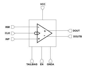
Voltage Latched Comparator
- A high-speed voltage clocked comparator with rail- to-rail outputs and no hysteresis.
- The typical propagation delay is 19ns while applying a differential input signal of 1mV over the offset voltage.
- The comparator operates with a supply voltage of 3.3V typical (VCC).
-
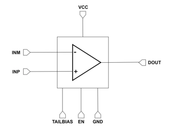
13ns High-Speed Comparator with no Hysteresis
- The TS_CMP_13ns_X8 is a high-speed comparator with no hysteresis and a propagation delay of 13ns while having a differential input signal of 25mV.
- The comparator consumes current of 350μA.
- The circuit features an Enable signal turning on/off the comparator.
-
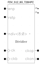
Frequency Divider
- Division ratio: any integer from 1 to 8/64/512/4096
- Maximum input frequency 2GHz – 10+GHz (A)
- Clock input and output signals are differential CMOS
- Control signals are single ended CMOS
