Memory Controller/PHY IP
Memory Interface IP cores support a wide range of memory types and standards, including DDR IP (Double Data Rate), GDDR IP (Graphics Double Data Rate), HBM IP (High Bandwidth Memory), and LPDDR IP (Low Power DDR), ensuring optimal performance in applications such as gaming, data centers, and mobile devices. NVM Express IP offers high-speed, low-latency storage interface for solid-state drives, while ONFI IP supports NAND flash memory communication. Additionally, SAS IP (Serial Attached SCSI) and SATA IP (Serial ATA) enable reliable, high-performance storage solutions, and SD/eMMC IP cores facilitate efficient data transfer for embedded systems.
All offers in
Memory Controller/PHY IP
Filter
Compare
1,246
Memory Controller/PHY IP
from
79
vendors
(1
-
10)
-
-
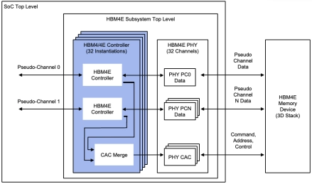
HBM4E Controller IP
- Supports HBM4/4E memory devices
- Supports all standard HBM4 channel densities (up to 32 Gb)
- Supports up to 16 Gbps/pin
- Refresh Management (RFM) support
-
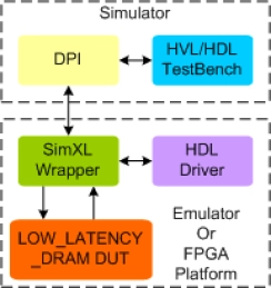
Low Latency DRAM Synthesizable Transactor
- Supports 100% of Low Latency DRAM protocol standard Low Latency DRAM specifications
- Supports 8 internal banks
- Supports all mode registers programming
- Supports programmable read latency and row cycle time
-
LPDDR5X/5/4X/4 combo PHY at 7nm
- Compliant with JEDEC JESD209-5B for LPDDR5X/5/4X/4 with PHY standards
- Delivering up to 8533Mbps
- DFI 5.1 specification PHY Interface Compliant
- Support up to 4 ranks
-
LPDDR5X/5/4X/4 combo PHY at Samsung SF5A
- Compliant for JEDEC standards for LPDDR5X/5/4X/4 with PHY standards
- DFI 5.1 specification PHY Interface Compliant
- Support up to 4 ranks
- x16 and x32 channel support

-
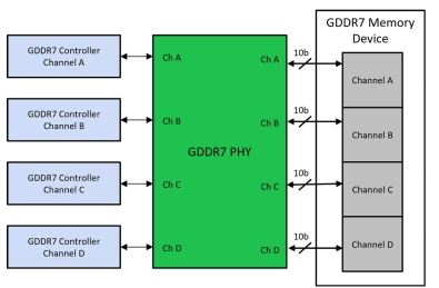
GDDR7 Memory Controller
- Supports up to 40 Gbps per pin operation
- 2.5 GHz CK4 clock
- 1.25 GHz controller clock
- Internal data path 32x memory width (i.e. 256 bits for 8-bit memory)
- Optimized for high efficiency and low latency across a wide range of traffic scenarios (random/sequential, short/long bursts, etc.)
- Optimized command sequence for highest bus utilization including per-bank refresh scheduling: single queue structure handles look-ahead activates/ precharges and read/write ordering for minimal latency
-
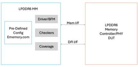
Simulation VIP for LPDDR6
- This Verification IP (VIP) is intended for modeling the upcoming JEDEC Low-Power Memory Device, LPDDR6 design specification.
- It provides a mature, highly capable compliance verification solution that supports simulation, formal analysis, and hardware acceleration platforms, making it applicable to intellectual property (IP), system-on-chip (SoC), and system-level verification.
-
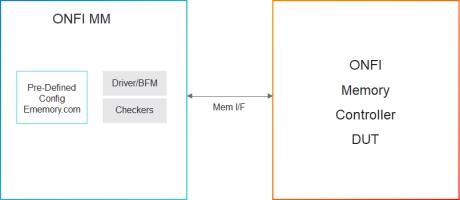
Simulation VIP for ONFi
- Hundreds of protocol and timing checkers to easily catch design bugs
- Hundreds of predefined configurations based on specific memory vendors' part numbers, datasheets, or generic JEDEC definitions available on ememory.com(opens in a new tab)
- Transaction and memory callbacks for all protocol, model states and device memory events
-
LPDDR6/5X/5 PHY V2 - Intel 18A-P
- The LPDDR6/5X/5 PHY IP enables ASICs, ASSPs, system-on-chips (SoCs), and system-in-package applications requiring high-performance LPDDR6, LPDDR5X, and/or LPDDR5 SDRAM interfaces operating at up to 14.4 Gbps
- With flexible configuration options, the LPDDR6/5X/5 PHY IP can be used in a variety of applications supporting LPDDR6, LPDDR5X, and/or LPDDR5 SDRAMs, precisely targeting the specific power, performance, and area (PPA) requirements of these systems

-
LPDDR6/5X/5 PHY V2 - TSMC N6
- The LPDDR6/5X/5 PHY IP enables ASICs, ASSPs, system-on-chips (SoCs), and system-in-package applications requiring high-performance LPDDR6, LPDDR5X, and/or LPDDR5 SDRAM interfaces operating at up to 14.4 Gbps
- With flexible configuration options, the LPDDR6/5X/5 PHY IP can be used in a variety of applications supporting LPDDR6, LPDDR5X, and/or LPDDR5 SDRAMs, precisely targeting the specific power, performance, and area (PPA) requirements of these systems
- LPDDR6 SDRAM’s combination of high bandwidth, capacity, low power, and cost effectiveness makes LPDDR6/5X/5 SDRAMs an attractive solution for traditional and new markets
- The LPDDR6/5X/5 PHY IP is designed to appeal to a variety of applications including: * Traditional mobile environments * Consumer products * Automotive solutions * Artificial intelligence * Data center applications
