Other
All offers in
Other
Filter
Compare
482
Other
from
30
vendors
(1
-
10)
-
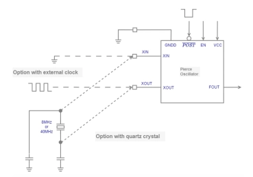
8MHz / 40MHz Pierce Oscillator - X-FAB XT018-0.18µm
- The TS_XOSC_40M_X8 is a 8MHz / 40MHz Pierce oscillator that generates a VCC-level logic square wave when a 8MHz / 40MHz quartz crystal is connected between its output XOUT and input XIN with external grounded load capacitors.
-
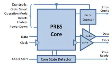
32Gbps, 31 order, Pseudo Random Bit Sequence Generator / Checker
- This unit generates and checks Pseudo Random Bit Sequence (PRBS) of 31 order, up to 32Gbps. Error count is accurate: no double counts or omissions regardless of error sequence or frequency of occurrence.
- Can be used as Generator, Checker or both. No inductors are used minimizing area and EM interference. Simple control interface, with low frequency asynchronous signals only.

-
32Gbps, 7/15/31 order, Pseudo Random Bit Sequence Generator/Checker
- PRBS order: 7, 15 or 31 based on formulas: X1=X6^X7; X1=X14^X15; X1=X28^X31
- Full bit rate at input and output up to 32Gbps
- Generator, Checker and Counter functions
- Accurate error count: no omissions or double counts
- Full rate CMOS differential input data, centered with half-rate CMOS differential clock
- Full rate CMOS differential output data, aligned with half-rate CMOS differential clock
-
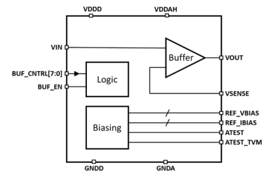
High Drive Strength Voltage Buffer on TSMC 16 FFC
- The ODT-OBF-ULP-DC-16FFCT is a voltage buffer with a high drive capability and is stable up to a 1nF output load.
- It can be used to daisy-chain voltages between different AFEs and different SoCs.
- The ODT-OBF-ULP-DC-16FFCT is powered by a 1.8V analog supply and a 0.8V digital supply.
-
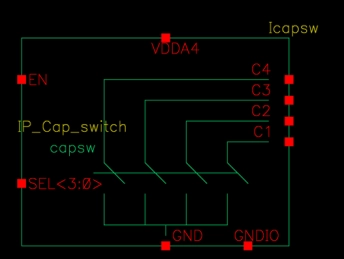
Quadruple Capacitor Switch
- The TS_SW_4Cap_X8 is a quadruple capacitor switch that is primarily used for resonator/transducer trimming.
- Large off-chip capacitors can be connected to the terminals C1 through C4: for example, 680pF (C4), 510pF (C3), 330pF (C2), 180pF (C1). When an NMOS switch is on, it pulls the terminal voltage down to ground through a low series drain-source resistance.
-
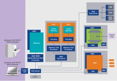
SLM SHS IP
- The SLM SHS IP is an automated hierarchical test solution for efficiently testing SoCs or designs using multiple IP/cores, including analog/mixed-signal IP, digital logic cores and interface IP.
- It significantly reduces test integration time by automatically creating a hierarchical IEEE 1500 network to access and control all IP/cores at the SoC level, and increases test quality of results (QoR), including optimizing test time and power through flexible test scheduling of IP and cores.
-
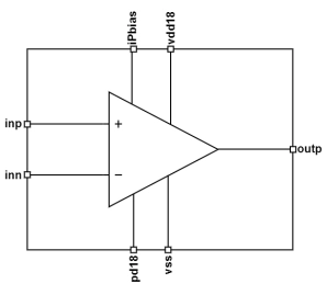
Special Purpose Low (Statistical) offset Operation Amplifier
- The WEAOPSPLO18PI18RO12M22G is a special purpose low offset buffer for bias generator that provides a buffered ouput for the Temperature Sensor
- The OpAmp deliberately exhibits systematic offsets to favor near zero Output Voltages
- It is Ideal for Temperature sensors with Rail – To – Rail Output that can go down to zero values.
-
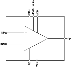
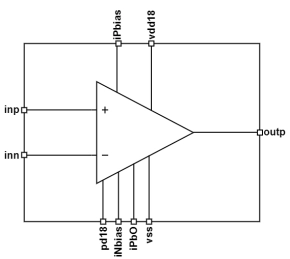
Rail to Rail Input and Output Operational Amplifier
- The WEAOPSP18RI18RO1F22G is a rail to rail input and rail to rail output folded cascode with rail to rail output gm stage with input offset control capability
- The opamp is ideal for ADC input buffers with offset control requirements for the ADC calibration.
-
Special Purpose Low offset Operational Amplifier
- The WEAOPSLOSP18NI18RO12M22G is a special purpose low offset buffer for bias generator that provides a buffered output for the bandgap voltage.The OpAmp deliberately exhibits systematic offsets to favor near zero Output Voltages
- It is Ideal for Power Detector and Temperature sensors with Rail – To – Rail Output that can go down to zero values.
-
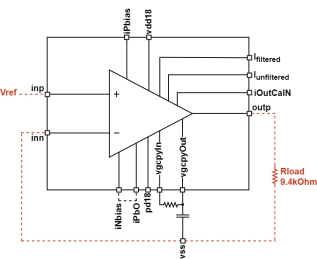
Special Purpose Low offset Operational Amplifier
- The WEAOPSLO18NI18RO12M22G is a special purpose low offset and low noise opamp
- The opamp architecture is two-stage Miller with RC compensation
- The opamp provides current outputs that copy the current flowing out of the main opamp output
- This feature allows easy poly current generation since the current copied at the current outputs will have a relation of Vref/Rload when the opamp is connected as a unity gain buffer with vref at its positive input