PCI IP
Welcome to the ultimate PCI IP hub! Explore our vast directory of PCI IP
All offers in
PCI IP
Filter
Compare
535
PCI IP
from
53
vendors
(1
-
10)
-
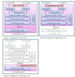
Configurable PCI Express 4.0 Link Controller
- Compliant with "PCI Express™ Base Specification, Rev. 4.0 Version 1.0"
- Compliant with "PHY Interface For the PCI Express, SATA, and USB3.1 Architectures"
-
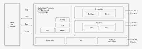
PCIe Gen4.0 PHY IP
- Best-in-class Power / Performance / Area competitiveness
- Compliant to PCIe 4.0 Base specification
- Supports lane configurations according to the user’s demands
- Supports data rates of 2.5GT/s, 5.0GT/s, 8.0GT/s and 16GT/s

-
PCIe Gen5/6 PHY IP
- Best-in-class Power / Performance / Area competitiveness
- Compliant to PCIe 5.0/6.x Base specification
- Supports lane configurations according to the customer’s demands
- Supports data rates of 2.5GT/s, 5.0GT/s, 8.0GT/s, 16GT/s, 32GT/s and 64GT/s (PAM4)
-
PCIe PHY and controller solution
- Brite 16Gbps PCIe PHY and controller solution provide high efficient interconnection that is optimized for PPA performance. The System can support short-reach or long-reach channels for plenty application scenarios.
- Brite PCIe controller to AXI architecture provides a high-performance, easy-to-use interconnect solution between PCI Express and the latest version of the AXI protocol. It inherits the leading architecture and features an AXI user interface with built-in DMA, compliant with the AMBA® AXI3 and AXI4 specifications.
-
PCIe 6.0 PHY, TSMC N3A x4 1.2V, North/South (vertical) poly orientation for Automotive, ASIL B Random, AEC-Q100 Grade 2
- Supports the latest features of PCIe 6.x and CXL 3.x specifications
- Supports PAM-4 signaling and up to x16 lane configurations with bifurcation
- Delivers more power efficiency across channels with unique DSP algorithms
- Enables near zero link downtime with patent-pending diagnostic features
-
PCIe Controller IP
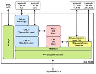
- The PCI Express® (PCIe®) Controller IP is a highly configurable, performance-optimized core designed for ASIC and FPGA integration.
- Supporting PCIe Gen1 through Gen6 at data rates up to 64 GT/s, the controller accommodates a wide range of link widths (x1–x16) and protocol features to meet the demands of next-generation SoC, networking, and high-performance computing platforms.
- The controller seamlessly interoperates with PIPE-compliant PHYs and supports multiple modes including Root Complex, Endpoint, Switch, and Dual-Mode operation.
-
PCIe Multi-Function Option for DMA IP Cores
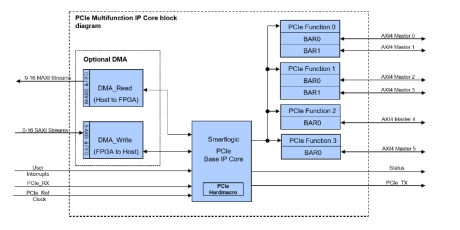
- The PCI Express specification allows endpoints that incorporate several physical PCIe functions that share the same PCIe connection. Such endpoints are called multi-function devices.
- The big advantage of a multi-function device is, that a separate device driver can be associated to each physical function.
- This simplifies driver development and maintenance significantly by separating the peripheral functions logically into different device drivers.
-
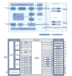
AXI Bridge for PCIe IP Core
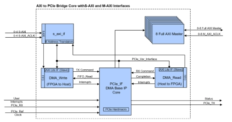
- The AXI Bridge for PCIe IP core is the IP solution with a powerful mix of multiple industry standard memory mapped AXI Interfaces.
- The AXI Bridge IP core translates the AXI4 memory read or writes to PCI-Express Transaction Layer Packets and translates PCIe memory read and write requests to AXI4 transactions.
- All interfaces support fully parallel operation without any interferences. Interfaces that are not required can be turned off individually and do not occupy logic resources.
-
Verification IP for PCIe
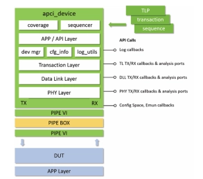
- Accelerated confidence in simulation-based verification of RTL designs with PCI Express (PCIe) interfaces: PCIe Gen2/3/4/5/6/7
-
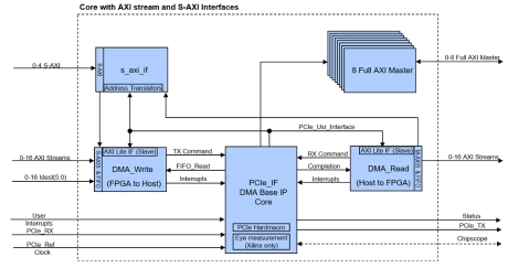
AXI Bridge with DMA for PCIe IP Core
- The AXI Bridge with DMA IP core is the ultimate PCIe DMA IP solution with a powerful mix of multiple industry standard AXI Interfaces.
- AXI Stream interfaces allow continuous data streaming from FPGA to Host or from Host to FPGA. S-AXI Memory mapped interfaces allow easy data access of remote memories in order to realize shared memory access or per to peer applications.
