DDR IP
DDR IP (Double Data Rate Interface) cores support high-speed data transfer for various types of DDR memory, including DDR3, DDR4, and DDR5, ensuring optimal performance for applications in computing, mobile devices, automotive systems, and embedded solutions. DDR IP cores offer features such as low latency, high bandwidth, and power efficiency.
All offers in
DDR IP
Filter
Compare
517
DDR IP
from
38
vendors
(1
-
10)
-
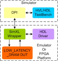
Low Latency DRAM Synthesizable Transactor
- Supports 100% of Low Latency DRAM protocol standard Low Latency DRAM specifications
- Supports 8 internal banks
- Supports all mode registers programming
- Supports programmable read latency and row cycle time
-
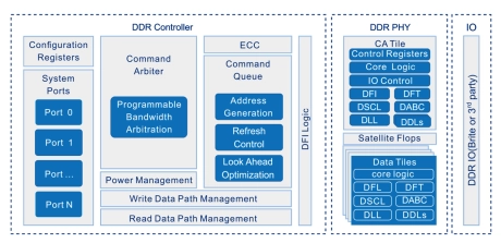
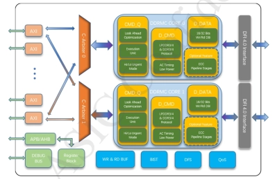
High Speed DDR Interface Solution
- Brite provides a complete DDR subsystem including not only controller, PHY and IO, but also corresponding tuning and configuration software. And this solution can support LPDDR2, DDR3, LPDDR3, DDR4 and LPDDR4/4x combo PHY with the data rate from 667Mbps to 4266Mbps.
-
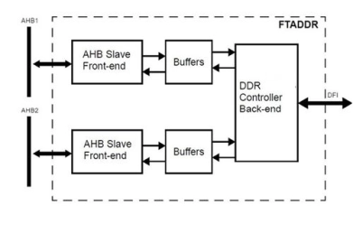
Fault Tolerant DDR2/DDR3/DDR4 Memory controller
- FTADDR is a memory controller for DDR2,DDR3 and DDR4 SDRAM memory devices.
- It uses a strong error correction code to achieve exceptional fault tolerance
-
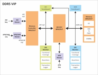
DDR5 LRRDIMM Verification IP
- Compliant to JEDEC DDR5 SDRAM Specification, Data Buffer & RCD Specification.
- Supports connection to any DDR5 Memory Controller IP communicating with a JEDEC compliant DDR5 Memory Model.
- Supports configurable SDRAM addressing of different sizes (x4, x8 and x16).
- Available in all memory sizes up to 64 Gb.
- Supports for all speed-grades/speed-bins.
-
DDR5 RDIMM Verification IP
- The DDR5 RDIMM Verification IP provides an effective & efficient way to verify the components interfacing with DDR5 RDIMM interface of an ASIC/FPGA or SoC.
- The DDR5 RDIMM VIP is fully compliant with Standard DDR5 specification from JEDEC.
- This VIP is a light weight with an easy plug-and-play interface so that there is no hit on the design time and the simulation time.

-
DDR6 Verification IP
- The DDR6 Verification IP provides an effective & efficient way to verify the components interfacing with DDR6 interface of an ASIC/FPGA or SoC.
- The DDR6 VIP is fully compliant with Standard DDR6 specification from JEDEC.
- This VIP is a light weight with an easy plug-and-play interface so that there is no hit on the design time and the simulation time.

-
DDR3 and DDR4 Controller and PHY on TSMC 12nm
- This DDR3/4 IP combo solution presented, is meticulously designed for high performance and low power consumption, utilizing sophisticated architecture and advanced technology.
- Fabricated in TSMC’s 12nm CMOS process, this solution includes both controller and PHY IPs, providing comprehensive support for DDR3 and DDR4 memory interfaces.
-
DDR5 MRDIMM PHY and Controller
- The DDR5 12.8Gbps MRDIMM Gen2 PHY and controller memory IP system solutions double the performance of DDR5 DRAM.
- The DDDR5 12.8Gbps design and architecture address the need for greater memory bandwidth to accommodate unprecedented AI processing demands in enterprise and data center applications, including AI in the cloud.
-
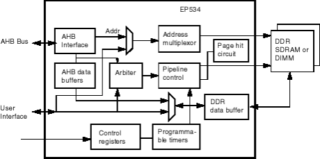
AMBA AHB Bus to DDR SDRAM Controller
- External pin reduction by transferring 2 bits of data per pin.
- Supports multiple external SDRAM banks.
- Automatic refresh generation with programmable refresh intervals.
- Self-refresh mode to reduce system power consumption.
- Standard delay cells or user provided DLL for DQ and DQS alignment.
-
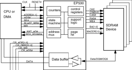
DDR SDRAM Controller
- Supports industry standard Double Data Rate (DDR) SDRAM.
- Designed for ASIC and FPGA implementations in various system environments.
- Programmable memory size and data width.
- Supports industrial standard 64Mbit, 128Mbit and 256Mbit DDR SDRAMs.