IP for Samsung
Welcome to the ultimate
IP
for
Samsung
hub! Explore our vast directory of
IP
for
Samsung
All offers in
IP
for
Samsung
Filter
Compare
259
IP
for
Samsung
from
27
vendors
(1
-
10)
-
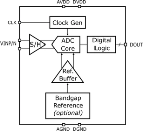
14-bit, 1200 MSPS Ultra Low Power ADC in 28nm CMOS
- 14-bit resolution, sampling rate up to 1200 MSPS
- Fully differential operation, fully specified from -40C to 125C
- Ultra low power dissipation
- Internal bandgap and voltage reference
-
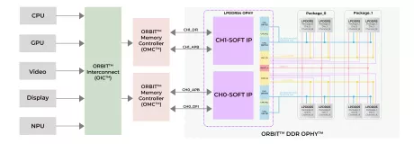
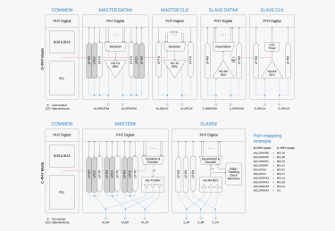
LPDDR5X/5/4X/4 combo PHY at Samsung SF5A
- Compliant for JEDEC standards for LPDDR5X/5/4X/4 with PHY standards
- DFI 5.1 specification PHY Interface Compliant
- Support up to 4 ranks
- x16 and x32 channel support
-
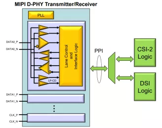
MIPI D-PHY Transmitter/Receiver for DSI/CSI-2 on Samsung 28nm FD-SOI
- Technology is Samsung 28nm FD-SOI 8M (6U1x_2T8x_LB).
- Supply voltage can be applied 1.1V for core voltage, 1.8V for IO voltage.
- Maximum data rate of each channel is 1.5Gbps at High-speed mode.
-
Intra-panel TX PHY IP
- The Intra-panel TX PHY IP is a low-power transmitter designed for COG (Chip-on-Glass) and COF (Chip-on-Film) display modules.
- It supports data rates up to 4.0Gbps, utilizing a DC-coupled differential pair and a push-pull current mode driver with 600mV swing and 6dB pre-emphasis, enabling high-speed and reliable panel-to-display communication.

-
DP and eDP TX/RX PHY IP
- eDP v1.5 compliant
- Supports for 1.62Gbps to Max 8.1Gbps data rate
- PSR, PSR2 supported for low power consumption ( FW_SLEEP, FW_STANDBY supported )
- Supports for eDP v1.5 feature such as AUX-less Link Training
-
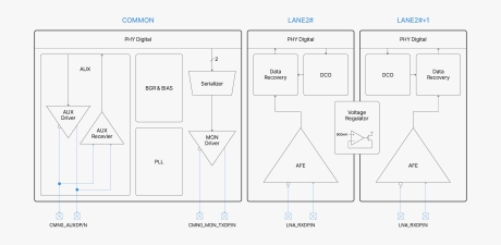
MIPI C/D-PHY Combo IP
- Compliant to MIPI D-PHY v3.0, C-PHY v2.1 specification
- Area efficient macro optimized for placement for dense SoC designs
- Support Uni-(TX or RX) and Bi-directional(TX and RX) mode
- Support emphasis architecture over lossy channel for TX
- Support equalize architecture over lossy channel for RX
-
20G MSS (Multi-standard SerDes) PHY
- Developing under SF4X CMOS technology (2025.06.30 MTO)
- Compliant to multiple standards, max datarate 20Gb/s
- Channel Configuration for Data Lanes: 1, 2 or 4 Data Lanes
- Reliable Ring OSC PLL based architecture for Low power consumption
-
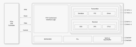
PCIe Gen4.0 PHY IP
- Best-in-class Power / Performance / Area competitiveness
- Compliant to PCIe 4.0 Base specification
- Supports lane configurations according to the user’s demands
- Supports data rates of 2.5GT/s, 5.0GT/s, 8.0GT/s and 16GT/s

-
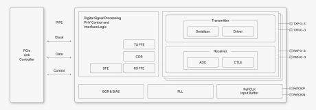
PCIe Gen5/6 PHY IP
- Best-in-class Power / Performance / Area competitiveness
- Compliant to PCIe 5.0/6.x Base specification
- Supports lane configurations according to the customer’s demands
- Supports data rates of 2.5GT/s, 5.0GT/s, 8.0GT/s, 16GT/s, 32GT/s and 64GT/s (PAM4)
-
100G SerDes PAM4 PHY
- The SERDES PHY IP delivers a high-performance, low-power solution for high-speed interfaces up to 112Gbps.
- It supports diverse applications including AI accelerators, data centers, 5G infrastructure, and automotive SoCs.
