Interface IP Cores
Interface IP cores are used to achieve communication between chips and external devices or other chips. Common interface standards include USB, PCIe, SATA, I2C, SPI, Ethernet, etc.
Explore our vast directory of Interface IP cores below.
All offers in
Interface IP Cores
Filter
Compare
3,398
Interface IP Cores
from
175
vendors
(1
-
10)
-
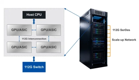
112G Multi-Rate SerDes
- Designed with a small footprint, ultra-low latency, and low power consumption, the 112G SerDes maximizes bidirectional memory access efficiency, reduces software complexity, and helps chip developers leverage existing Ethernet infrastructure to significantly lower Total Cost of Ownership (TCO).
- Featuring IEEE 802.3-compliant Forward Error Correction (FEC), 35dB ultra-high channel loss compensation, and adaptive high-speed equalization technologies (CTLE, FFE), it provides full-cycle link protection—from error correction to pre-warning—enabling highly compatible, stable, and efficient chip-to-chip connectivity solutions.
-
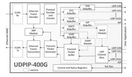
400G UDP/IP Hardware Protocol Stack
- Implements a UDP/IP hardware protocol stack that enables high-speed communication over a LAN or a point-to-point connection.
- Designed for standalone operation, the core is ideal for offloading the host processor from the demanding task of UDP/IP encapsulation and enables media and data streaming with speeds up to 400Gbps in ASICs even in processor-less SoC designs.
-
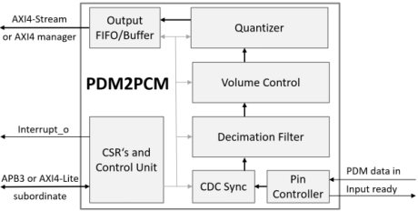
PDM Receiver/PDM-to-PCM Converter
- This PDM2PCM is a configurable audio interface core that converts a mono or stereo Pulse Density Modulation (PDM) stream into standard Pulse Code Modulation (PCM) format.
- PCM output widths are programmable from 2 to 32 bits, and all standard audio sampling rates are achievable via an adjustable Oversampling Ratio (OSR) from 32x to 256x.
-
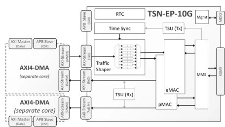
TSN Ethernet Endpoint Controller 10Gbps
- The TSN-EP-10G implements a configurable controller meant to ease the implementation of endpoints for networks complying with the Time Sensitive Networking (TSN) standards
- It integrates hardware stacks for timing synchronization (IEEE 802.1AS-2020) and traffic shaping (IEEE 802.1Qav and 802.1Qbv), frame-preemption (IEEE 802.1Qbu and IEEE 802.3br) and a low-latency Ethernet MAC.
-
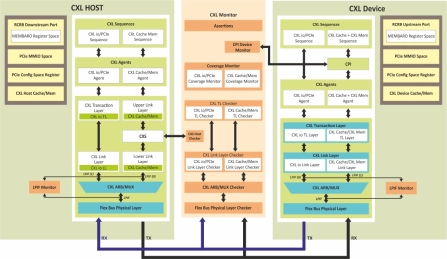
CXL 4 Verification IP
- Compliant with the CXL 4, 3.2, 2.0 & 1.1 Specifications.
- Support for all three protocols CXL.IO, CXL.CACHE & CXL.MEM including all CXL device types
- Support for PCIE Mode & Alternate Protocol Negotiation for CXL Mode
- Support for 256B flit in 128GT/s with PCIe Gen 6 as well as 64/32/16/8 GT/s speeds with backward compatibility.
-
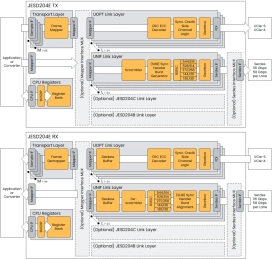
JESD204E Controller IP
- The JESD204E Controller IP from Chip Interfaces is an early adopter’s version of the upcoming revision of the JEDEC standard for Serial Interface for Data Converters.
- The JESD204-E IP core supports the UCIe Optimized Link Layer, a dedicated mode to run JESD over UCIe Modules with Line rates up the 64Gbps per bump, and a JESD204D backwards compatible mode called the Unified Link Layer with line speeds up to 116Gbps with PAM4 and 58Gbps with NRZ and full FEC support.
-
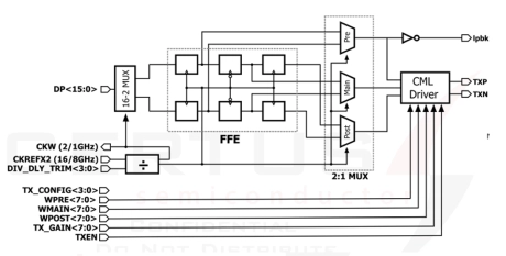
32Gbps SerDes PHY in GF 22nm
- This 32Gbps SerDes PHY is implemented in GlobalFoundries 22FDX CMOS technology and provides a high-performance, protocol-agnostic serial interface for advanced mixed-signal and high-speed digital SoCs.
- The PHY is architected as a modular design consisting of a low-jitter clock multiplier, a half-rate transmitter with digitally programmable feed-forward equalization, and a configurable CTLE-based receiver with digital clock-and-data recovery, supporting both 16 Gbps and 32 Gbps operation.
-
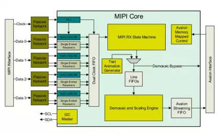
MIPI CSI2 Receiver
- Provides Compatible MIPI D-Phy v1.1 physical layer using FPGA LVDS/LVCMOS IO and passive network
- Supports CSI-2 protocol for unidirectional data transfer
- Compatible with D-PHY Configured for 1 clock and 4 data lanes
- Intended for per-lane clocks rates up to 1 Gbps, depending on device speed grade
-
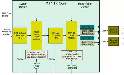
MIPI CSI2 Transceiver
- Provides Compatible MIPI D-Phy v1.1 physical layer using FPGA LVDS/LVCMOS IO and passive network
- Supports CSI-2 protocol for unidirectional data transfer
- Compatible with D-PHY Configured for 1 clock and 1 data lane
- Intended for per-lane clocks rates up to 1 Gbps, depending on device speed grade
-
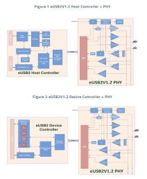
eUSB2V1.2 Controller + PHY IP
- eUSB2 can support USB high-speed, full-speed, and low-speed operation, as well as the USB 2.0 L1/L2 link power management requirements. In addition, eUSB2 requires no change to the existing USB 2.0 software programming model.
- eUSB2 also uses the same two data line configurations, eD+ and eD- as USB2 D+ and D-. Vbus and power delivery are not impacted by eUSB2.