UALink™ Shakes up the Scale-up AI Compute Landscape
OCP Global Summit 2024 in San Jose, CA featured a slew of exciting announcements. The x86 Ecosystem Advisory Group stirred up much buzz.
However, Kurtis Bowman and J Metz's standing room-only presentation on Ultra Accelerator Link™, a new standard, caught the industry's attention as it has the potential to shake up the semiconductor ecosystem for AI compute.
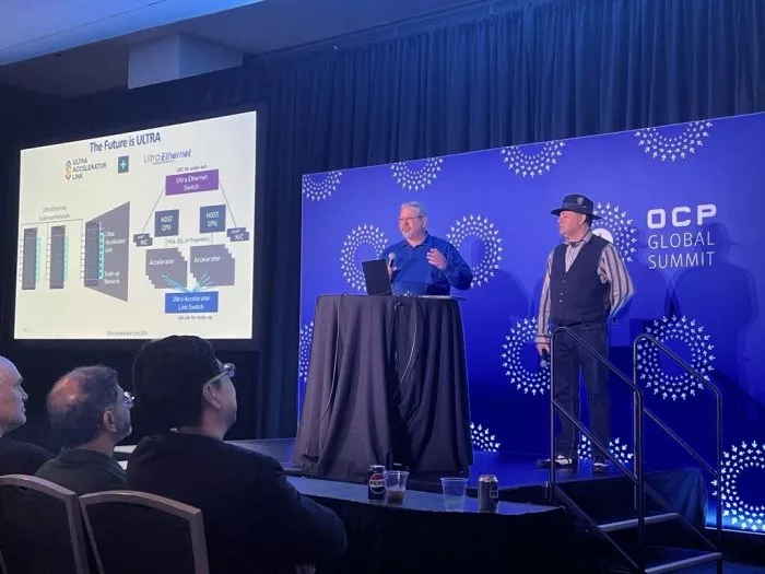
Kurtis Bowman and J Metz at OCP Global Summit
Motivation for scale-up and a standard-based solution
Transformers have been at the core of the generative AI revolution. When Vaswani et al [1] published their seminal paper on transformer architecture, Attention Is All You Need, they shared results using 8 GPUs to demonstrate improvements in language translation capabilities using their models.
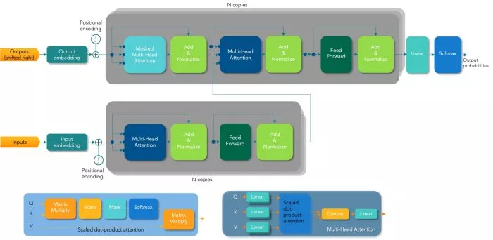
Figure 1: Transformer architecture [1]
In the years that followed, GPU, accelerator, and xPU architectures have evolved to keep up with the rapid pace of AI use cases and application evolution that brought ChatGPT, DALL-E and Midjourney to the common lexicon. This torrid growth cycle has come at a cost: model size, parameters, compute and other associated costs have risen exponentially. Figures 3 and 4 below show the dramatic growth from GPT-1 to GPT-4 (based on public data) from approximately 117M parameters to 1.7 trillion parameters while the processing required surged from 10s of petaFLOPS to billions of petaFLOPS across model generations.
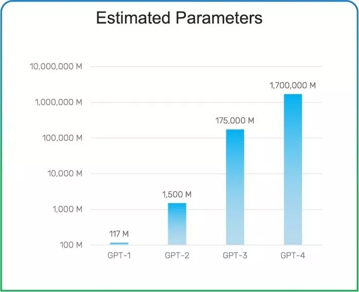
Figure 1: Growth in number of GPT LLM parameters (public data)
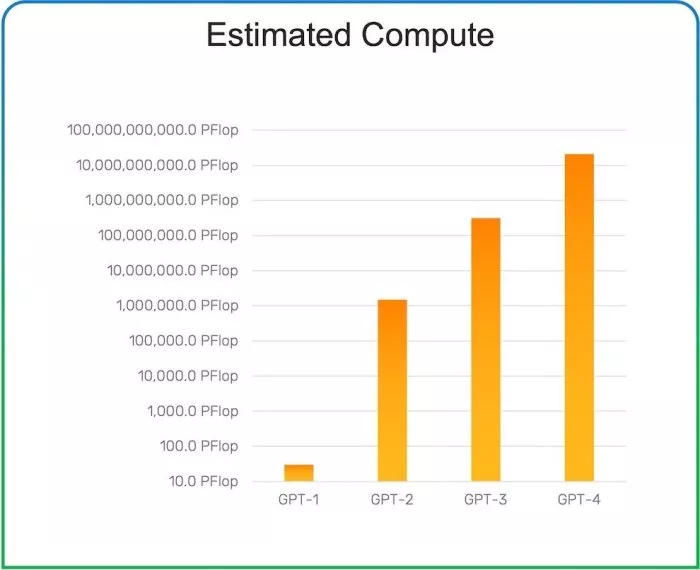
Figure 2: Exponential growth of compute requirements for GPT LLMs (public data)
The core of the transformer architecture is based on matrix multiplication and vector operations: a set of computations that GPUs are extremely well suited for. One limitation with standard off-the shelf GPUs is that they have proprietary interfaces for GPU-to-GPU communication designed for general traffic requirements (or in some cases based on past datasets).
With the growth in parameter sizes, model and data partitioning became essential to solve these problems with available physical resources in a reasonable time. Essentially, we need to scale-up an accelerator and its local memory to a set of connected accelerators such that the attached memories (typically HBM) are accessible robustly with low-latency, leaving coherency to software. In highly simplified terms, we have created a virtual super-accelerator or super-GPU with a much larger memory that is essentially a large flat space that is accessible by any accelerator.
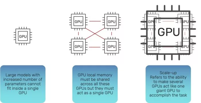
Figure3: Scaling up with multiple accelerators (Based on Kurtis Bowman's talk at OCP Global Summit '24)
Custom accelerator designs rapidly emerged to address unique system solutions in the generative AI space. However, these custom accelerators face challenges when interfacing with proprietary standards within the walled garden of current solutions.
Industry leaders collaborate to form the consortium
Industry stalwarts banded together to propose an open standard for accelerator-to-accelerator interfaces that addresses this problem. The Ultra Accelerator Link Consortium (www.ualinkconsortium.org) was formed early 2024 and formally incorporated in October. UALink has articulated a very focused mission from the outset:
The UALink Consortium is an open industry standard group formed to develop technical specifications that facilitate direct load, store, and atomic operations between AI Accelerators (i.e. GPUs), focused on low latency/high bandwidth fabric for hundreds of accelerators in a pod and on simple load and store semantics with software coherency. The UALink 1.0 Specification taps into the experience of the Promoter Members developing and deploying a broad range of accelerators. (UALink Consortium website)
This laser focus on accelerator-to-accelerator communication for memory operations allows the UALink Consortium to concentrate its energies on solving a critical problem while also relying on other well-established interface standards to accomplish tasks they already perform effectively.
Scale-up in the AI datacenter and AI factory
UALink optimizes xPU-to-xPU memory communication across accelerators in a pod, either directly connected or through a fully connected high-radix switch. Accelerators are typically attached to their host processor using a standard high-speed serial interface such as PCIe® or CXL®.
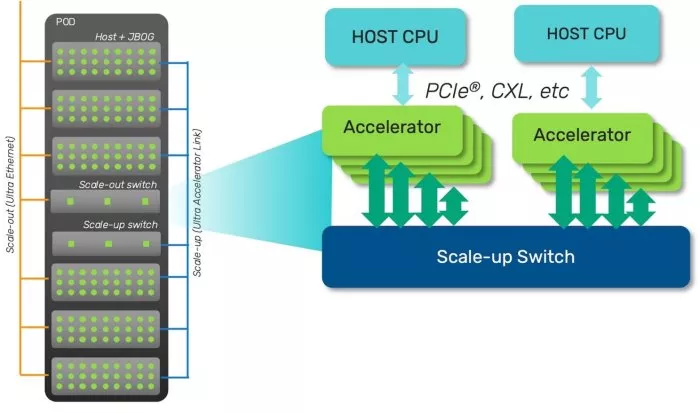
Figure 4: UALink scale-up pod
Expansion across pods relies on an optimized version of ethernet called Ultra Ethernet, driven by the Ultra Ethernet Consortium, another standard formed by leading hyperscalers to accelerate datacenter ethernet (essentially a replacement for bulk transfers that rely on remote DMA/RoCE today).
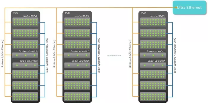
Figure 5: UALink pod expansion
The future is Ultra. -- Kurtis Bowman and J Metz
Figure 6 shows a system interconnectivity diagram highlighting the various protocols interacting with a system node that is UALink capable.
- xPU-to-xPU traffic within a pod is through the UALink scale-up network using a UALink switch
- Scale-out (pod expansion) is over Ultra Ethernet. This network is used for OS operations, memory management, and sharing information across hosts and remote accelerators.
- Host-xPU traffic is managed using a standard high-speed serial interface such as PCIe® or CXL®. The hosts convey job information to the xPUs, memory mapping information etc over the local interface to the xPU.
- The front-end LAN/WAN connectivity is over standard ethernet
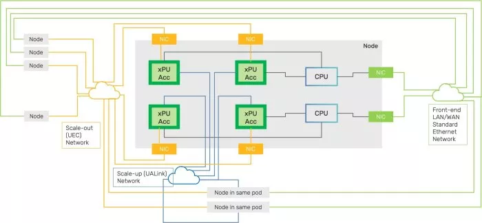
Figure 6: UALink Node in a system and its interaction with other standards
UALink Specification
The initial set of promoters/board members that worked on the UALink specification drew on their experience with AI models and partitioning to determine what constituted the key features defining the 1.0 specification.
The public specification calls for up to 1024 hosts in a pod. The other piece of information that has been shared publicly is that the physical layer will be based on the IEEE 802.3dj standard at the 200Gb/s rate.
Consortium membership is open now. Contributor members can access the specification in Q4 while the public will be able to access it in 2025.
Cadence Design Systems is a proud member of Ultra Accelerator Link Consortium and Ultra Ethernet Consortium and looks forward to participating in this space. It's an exciting time for the semiconductor industry especially those working towards building an AI ecosystem. UALink promises to shake things up.
Related Semiconductor IP
- UALink Controller
- Simulation VIP for UALink
- UALink PCS IP Core
- Verification IP for UALink
- UALink IP Solution
Related Blogs
- Powering Scale Up and Scale Out with 224G SerDes for UALink and Ultra Ethernet
- Verification of UALink (UAL) and Ultra Ethernet (UEC) Protocols for Scalable HPC/AI Networks using Synopsys VIP
- Is The ARM-Globalfoundries Link Significant?
- Link Training: Establishing Link Communication Between DisplayPort Source and Sink Devices
