Driving the Future of High-Speed Computing with PCIe 7.0 Innovation
Escalating compute processing demands from generative and agentic AI applications have spurred a massive AI infrastructure buildout, and the need for faster and more efficient data transfer capabilities has never been greater. Protocol standards and speeds are advancing rapidly to boost productivity and efficiency for high-performance computing (HPC), AI training, and other applications, with the arrival of PCI Express (PCIe) 7.0 being the latest example. Coinciding with the availability of the PCIe 7.0 version 1.0 specification, the industry's most advanced PCIe 7.0 subsystem solution is available now from Cadence, giving SoC constructors for HPC and AI/ML applications another tool in their toolbox of high-speed protocol IP.
Featuring a DSP-based PHY and a feature-rich companion controller, the Cadence subsystem solution for PCIe 7.0 is designed specifically to meet the increasing data transfer demands of next-generation AI training and HPC systems. Early adopters of Cadence IP for PCIe 7.0 can access design kits now.
Advancing Performance with Cadence IP for PCIe 7.0
The 3nm PCIe 7.0 PHY from Cadence is a high-performance NRZ/PAM4 SerDes multi-protocol PHY that is compliant with the latest PCIe 7.0 specification. It delivers industry-leading performance of 128GT/s while achieving significant efficiency improvements in power and area utilization. With its high-performance, low-latency architecture and low power consumption, this IP is perfectly suited for high bandwidth, performance-critical applications in AI/ML, HPC, data communications, networking, and storage systems.
The feature-rich controller IP supports all the new PCIe 7.0 features while maintaining full compatibility with prior versions of the specification. The highly scalable and configurable architecture supports a maximum aggregate bandwidth of 512GB/s bi-directionally.
The fully integrated subsystems are silicon-tested in a subsystem test chip, which enables Cadence to validate the PHY and controller functions at the system level and perform rigorous compliance and stress tests to ensure universal interoperability and reliability. As part of the PCIe subsystem IP delivery, Cadence also provides verification IP and a simulation testbench to streamline hardware integration, as well as a software stack that allows customers to begin infrastructure development ahead of silicon availability.
"Designing for efficient data movement via high-speed I/O interfaces is critical given the cost to move data," said Marc Loinaz, vice president of research and development in the Silicon Solutions Group at Cadence. "With the lowest power consumption in the market as validated by our customers, Cadence's PHY and controller IP for PCIe 7.0 enable them to develop extremely power-efficient SoCs that contribute to more sustainable data centers while achieving long-reach performance requirements with best-in-class design margins for system robustness. With our multi-lane subsystem-on-a-chip solution, our customers can achieve IP compliance in form factors that match their target applications, allowing them to focus their critical resources on SoC differentiation."
Cadence Sets New Standard for Power-Efficient PCIe 7.0 Solutions
The Cadence IP for PCIe 7.0 has demonstrated exceptional performance and reliability, enabling early customers to design cutting-edge solutions featuring next-generation PCIe technology.
A collaborative ecosystem built on open standards is key to driving innovation and enabling the seamless adoption of new technologies across the industry.
"Intel is committed to fostering industry-wide innovation and supporting open standards like PCI Express to help customers address the most demanding data center workloads," said Debendra Das Sharma, Senior Fellow and Chief I/O Architect, Intel. "We look forward to working with Cadence, and the broader ecosystem, to help ensure interoperability for future solutions that pave the way for advancements that meet the evolving needs of the industry."
"Cadence showcased the robustness of their 128GT/s PCIe 7.0 PHY interoperating with Luxshare LPO Module OSFP 800G DR8 connector," said Vincent Zeng, general manager of Optoelectronics, Luxshare Precision Industry Co. Ltd. "This was the world's first stable demonstration of 128GT/s TX and RX over off-the-shelf optical connectors, making it the highlight of PCI-SIG DevCon 2024."
"Consistent with previous testing, Cadence's PHY for the PCIe 7.0 specification demonstrated robust performance in electrical tests using our DPO70000SX ATI performance oscilloscope," said Javier Irazola, General Manager, Performance Instruments at Tektronix Inc. "We're proud to support Cadence's innovative work at the forefront of high-bandwidth, hyperscale SoC IP. Their strong track record at PCI-SIG compliance events continues to inspire confidence in their solutions and in the broader PCIe ecosystem."
Cadence Continues to Expand Its Advanced IP Portfolio
The Cadence IP for the PCIe 7.0 specification is the newest addition to Cadence's high-performance IP portfolio—featuring 112G, 224G, D2D, and advanced memory IP—and is optimized for chiplet-based architectures and subsystem solutions that accelerate AI and HPC workloads.
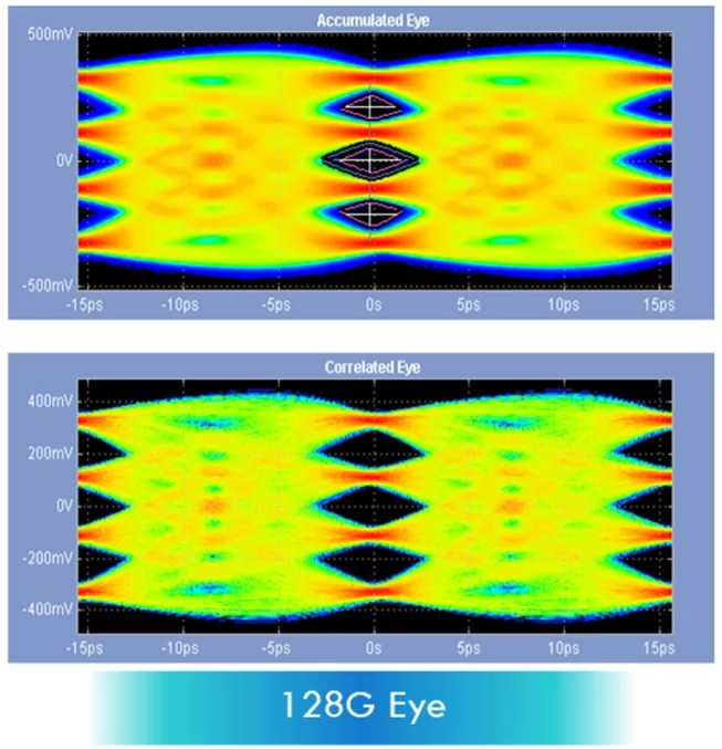
For a more in-depth look into this topic, check out our two demos at PCI-SIG DevCon 2025. The first will demonstrate PCIe 7.0 over optics in an advanced FinFET process, featuring a 128G TX eye using Luxshare LPO, while the second will highlight PCIe 7.0 readiness in the same process with a 128G TX eye.
Learn more about the Cadence IP for PCIe 7.0 specification, or watch Cadence Showcases World's First 128GT/s PCIe 7.0 IP Over Optics.
Related Semiconductor IP
- PHY for PCIe 7.0 and CXL
- PCIe 7.0 Controller with AXI
- PCIe 7.0 Switch
- PCIe 7.0 Retimer Controller with CXL Support
- PCIe 7.0 Controller
Related Blogs
- The Future of PCIe Is Optical: Synopsys and OpenLight Present First PCIe 7.0 Data-Rate-Over-Optics Demo
- Cadence Leads the Way at PCI-SIG DevCon 2025 with Groundbreaking PCIe 7.0 Demos
- Maximizing the Usability of Your Chip Development: Design with Flexibility for the Future
- The Power of Shifting Left: Cadence Accelerating Innovation with Arm
Latest Blogs
- Area, Pipelining, Integration: A Comparison of SHA-2 and SHA-3 for embedded Systems.
- Why Your Next Smartphone Needs Micro-Cooling
- Teaching AI Agents to Speak Hardware
- SOCAMM: Modernizing Data Center Memory with LPDDR6/5X
- Bridging the Gap: Why eFPGA Integration is a Managed Reality, Not a Schedule Risk