Cadence Leads the Way at PCI-SIG DevCon 2025 with Groundbreaking PCIe 7.0 Demos
As we move through 2025, the momentum generated by Cadence continues to energize the PCIe ecosystem. At the 2025 PCI-SIG Developer's Conference in Santa Clara, CA, Cadence delivered a commanding presence with industry-first demonstrations, deep technical insights, and a complete IP solution for PCIe 7.0 tailored for the demands of HPC and AI.
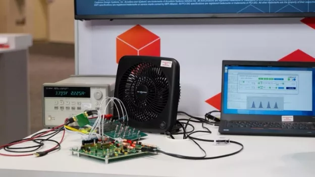
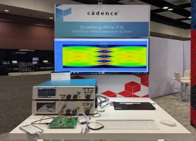
128 GT/s PCIe 7.0 Optical Demo
Cadence demonstrated a stable and high-performance 128 GT/s PCIe 7.0 TX and RX link operating over off-the-shelf, non-retimed linear optical connectors. The setup maintained a consistent pre-FEC BER of approximately 1E-8—well below the PCIe 7.0 specification threshold of 1E-6—throughout two full days of continuous operation. This real-world demonstration highlighted a robust, low-latency, and power-efficient solution with ample margin for RS FEC.
Highlighting the broader impact of this achievement, Vincent Zeng, general manager of Optoelectronics at Luxshare Precision Industry Co. Ltd., remarked, "This was the world's first stable demonstration of 128GT/s TX and RX over off-the-shelf optical connectors, making it the highlight of PCI-SIG DevCon."
This demo underscores the growing importance of Linear Pluggable Optics (LPO) in AI/ML data center architectures, where traditional DSP-based optical modules hit power and latency walls. Cadence's IP enables LPO solutions offering a compelling alternative—lower power, lower latency, and lower cost.
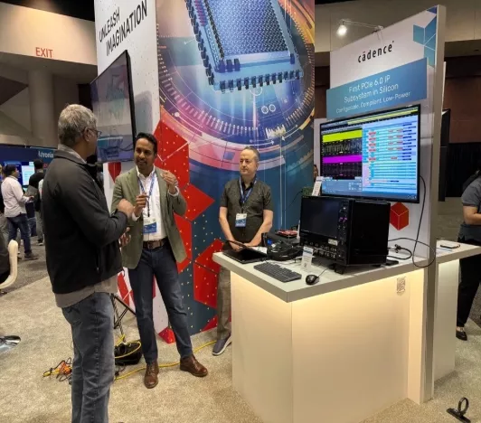
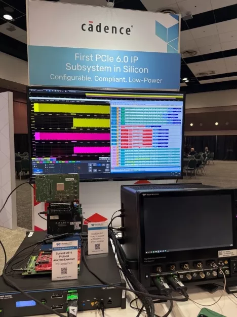
Deep PCIe Visibility with Teledyne LeCroy CrossSync PHY
In a powerful collaboration, Cadence's RP/EP back-to-back subsystem demo for PCIe 6.0 seamlessly interoperated with Teledyne LeCroy's CrossSync PHY Test Solution. CrossSync PHY captures live traffic of a PCIe 6.0 link using a Teledyne LeCroy WaveMaster 12bit, 320GS/s real time oscilloscope and a Teledyne LeCroy M616 PCIe 6.0 Protocol Analyzer/Exerciser. The Cross Sync PHY software displays a time-synchronized view of both the electrical waveforms as well as the protocol records into a single, time-correlated interface—providing unmatched insight into link behavior and accelerating root-cause analysis.
This joint demonstration showcased the performance and interoperability of both Cadence's high-bandwidth SoC IP subsystem and Teledyne LeCroy Test Tools, showing how customers can solve issues faster and improve time to market.
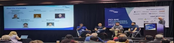
Thought Leadership: Deep Dive into PCIe Security and Scalability
Cadence's Anish Mathew made a strong impression during the PCI-SIG Marketing Work Group panel discussion, where he shared thoughtful insights into the architectural innovations Cadence has implemented to support evolving PCIe standards. He did an excellent job addressing a range of complex questions, including the roles of TDISP, DOE, and IDE in securing data over the PCIe bus, the distinctions between SIOV and SRIOV, and how PCIe switches can enhance AI application performance.
Cadence IP for PCIe 7.0 128GT/s in 3nm for HPC/AI
To meet the demands of next-gen computing, Cadence announced its solution for PCIe 7.0 IP, purpose-built for HPC and AI workloads. This includes:
- Protocol and electrical testing with real-world system interoperability
- Support for linear optics, enabling high-throughput, low-latency links across distributed data centers
This subsystem approach reduces risk in SoC design and accelerates time to market for customers building cutting-edge AI and data center solutions.
Summary
Cadence continues to set the pace in PCIe innovation. From PCIe 3.0 to 7.0, we've consistently delivered complete, compliant, and high-performance IP subsystems. With our latest solutions for PCIe 7.0, we're enabling the next generation of AI, HPC, and data center SoCs—faster, smarter, and more efficient than ever before.
Cadence is proud to be part of the PCI-SIG community and looks forward to what's next.
Learn more about Cadence's solutions for PCIe.
Related Semiconductor IP
- PHY for PCIe 7.0 and CXL
- PCIe 7.0 Controller with AXI
- PCIe 7.0 Switch
- PCIe 7.0 Retimer Controller with CXL Support
- PCIe 7.0 Controller
Related Blogs
- Cadence Demonstrates Complete PCIe 7.0 Solution at PCI-SIG DevCon 24
- Video: Cadence Demonstrates PCIe Gen3 Silicon at PCI-SIG Dev-Con (SAS RAID Controller)
- Industry's First Adopted VIP for PCIe 7.0
- Progressing on Track: PCIe 7.0 Specification, Version 0.7 Now Available for Member Review
Latest Blogs
- Area, Pipelining, Integration: A Comparison of SHA-2 and SHA-3 for embedded Systems.
- Why Your Next Smartphone Needs Micro-Cooling
- Teaching AI Agents to Speak Hardware
- SOCAMM: Modernizing Data Center Memory with LPDDR6/5X
- Bridging the Gap: Why eFPGA Integration is a Managed Reality, Not a Schedule Risk