An Effective way to drastically reduce bug fixing time in SoC Verification
By Sandeep Vaniya, eInfochips
Introduction
Many times we are not aware of very useful EDA tool options which are already available. Even if such options are very well documented, we don't look at them and try them [I partly agree that tool supports MANY options and trying/understanding them is time consuming and boring]. But some options are very useful and if you know them, it makes job of design engineer and/or verification engineer very easy.
Here, I am going to talk about one very powerful and useful VSIM option of QuestaSim. It is VCDSTIM option of VSIM. As per Mentor Graphics Corporation, people didn’t understand the value of this powerful option in bug hunting though it is already in the tool for so long.
[Note: VSIM is last step of 3 step (vlog => vopt => vsim) simulation flow of QuestaSim].
Details of VCDSTIM option
VCDSTIM is one of the options of VSIM of QuestaSim. Here are the details of this option as described in QuestaSim User Manual.
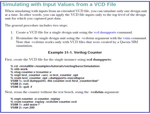
From description, I am sure you understood what this option does. Using it, you can drive module signals directly from VCD file.
Mostly, we drive DUT signals from Test Bench [through BFMs] and use VCD file to see them in the waveform. But this option utilizes VCD in completely different way. It takes data from VCD file to drive DUT signals. Isn't it great?
This option doesn't restrict you to drive IO [Input/Output/Inouts] of ANY INTERNAL module of the design.
Advantages of using VCDSTIM option
- VCDSTIM option can make debugging of SoC very easy.
- It can also drastically reduce the simulation time spent in locating and correcting the bug.
- It can also guarantee reproducing the design bug in the randomization based verification environment [VE] where sometimes it is very difficult to reproduce the bug found with particular random seed due to changes being made in the environment.
Now let me tell you how this option will help in saving time in fixing the bug.
Application of VCDSTIM
Consider that you are working on big SoC design which involves micro processor, multiple AHB layers, APB layer, AXI layer, various design IPs like Ethernet, USB, SATA, Flash Controller, DMA, Interrupt Controller, L2 Cache Controller, PCIe, GPIOs, I2C, SPI, various bridges like AHB to AHB bridge, AHB to APB bridge, AHB to AXI, AXI to AHB, etc, etc.. [This data is from one of the SoC product of Maxim Semiconductor which eInfochips have verified].
Let’s consider during simulation, some bug in particular IP or particular subsystem/block/module is found. So you report this bug to designer.
Designer look at the waveform, log, etc. and try to locate the issue. He fixes something in the design and re-run simulation. But bug is still not resolved. He again applies some more fixes but bug continues. [Note that for such a big SoC design, simulation time is very large in terms of hours.].
So, designer is getting frustrated, not because of number of iterations he is doing, but due to time spent in simulating each iterations [because each time he is simulating entire SoC design, applying stimulus from SoC Test Bench Top]. In such case, most designer strives to reproduce same issue in their local IP level/module level Test Bench to avoid waiting for so long for SoC simulation to complete. But for each IP, they might not have local Test Bench and it also not guaranteed to generate same scenario in local Test Bench. Even if local IP level Test Bench is available they need to spend time in figuring out HOW to REPRODUCE the issue and then WRITE TEST for the same [By this time, designer has still not started looking at the issue as he is busy in just REPRODUCING the issue in local Test Bench].
Having described this very common, time consuming and critical problem in verification of big SoC design, let’s see how VCDSTIM can be helpful here.
In this case, once it is confirmed that issue is inside particular IP or particular sub-system/block/module, one can generate VCD file only for that sub-system/block/module. And then re-run the simulation with VCDSTIM option giving VCD file, just generated.
- This simulation using VCDSTIM will drive same stimulus to particular module which was driven from SoC Test Bench Top earlier.
- This simulation [refer to VCDSTIM command line option description mentioned above carefully] is Not running at SoC Test Bench Top but at particular module top only.
- Simulation time spent in other Verification IP [VIP] components, BFMs, Test Bench, etc. will also reduce to zero as they will not be simulated.
This will drastically reduce simulation time as stimulus is only applied to particular module as opposed to entire SoC Top and at the same time it ensures that same stimulus [as in SoC Top] is applied to the suspected design module.
Designer can afford multiple iterations in locating and correcting the issue in this case as simulation time reduced drastically. Also he can start focusing on the bug directly instead of spending time in reproducing the issue in local Test Bench.
In this case, no matter how much randomization is changed or VE code is changed, stimulus will not change. So, bug will be guaranteed to get reproduced, irrespective of changes in the VE or randomization scheme.
The only thing you need to make sure is to LOCATE the sub_system/block/module which is responsible for bug.
Simulation time will be improved by factor which will be inversely proportional to size of the module [in comparison with size of entire design] in which bug is found.
Block diagram of stimulus
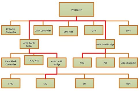
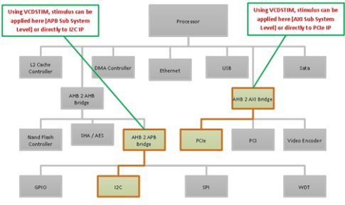
Following diagrams shows pictorial view of what I have described above.
Diagram shown below is depicting two scenarios where in one scenario Bug related to I2C is found while in other scenario Bug related to PCIe is found. This is showing normal stimulus coming from processor.
Following diagram shows stimulus using VCDSTIM.
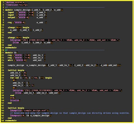
Sample Code showing working of VCDSTIM option
Having described details and application of VCDSTIM option, let’s see how this option works.
Refer to following snapshot.
Here you can see the code for sample_design [Verilog code for adder] and Test Bench.
In the Test Bench, sample_design.vcd file is created in the initial block [This VCD file will be used in VCDSTIM option]. VCD for particular module can also be created using “vcd dumpports” option of VSIM.
In other initial block, stimulus is applied to sample_design.
Display messages are printed from both Test Bench and sample_design module [This will distinguish what will happen in the simulation WITH VCDSTIM option].
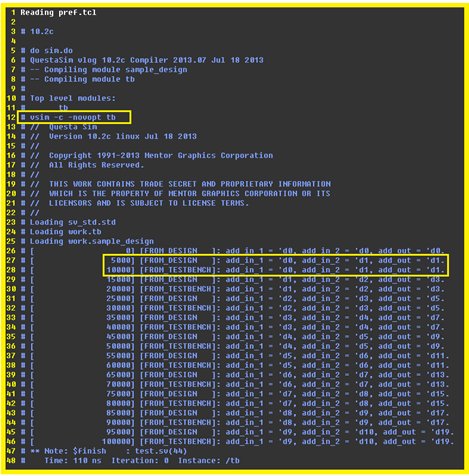
Following snapshot shows the simulation results without VCDSTIM option.
You can notice the Display messages from Test Bench as well as sample_design module are printed.
This simulation will generate the sample_design.vcd as entire Test Bench is simulated here.
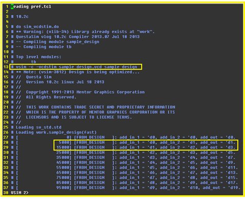
Following snapshot shows simulation result WITH VCDSTIM option using sample_design.vcd generated in earlier simulation.
You can notice that Display messages from Test Bench are no longer printed as ONLY sample_design module is simulated [Test Bench is bypassed].
Display messages from ONLY sample_design are printed.
Compare the values of adder inputs and output in print messages in both simulations. They are same in both simulations which means same stimulus is applied using VCDSTIM option.
In this example, I have compiled both Test Bench and sample_design WITH VCDSTIM option. But, it is also possible to compile ONLY sample_design while using VCDSTIM option. This will be very helpful in big design where compile time is also very significant. Just compiling particular module [which is supposed to be simulated using VCDSTIM], you will save time spent in compilation as well.
I hope this will enlighten your SoC debugging skill and help in design/verification activity you are doing!!!
Feel free to contact me in case of any query on my email id: sandeep.vaniya@gmail.com
Related Semiconductor IP
- ReRAM NVM in DB HiTek 130nm BCD
- UFS 5.0 Host Controller IP
- PDM Receiver/PDM-to-PCM Converter
- Voltage and Temperature Sensor with integrated ADC - GlobalFoundries® 22FDX®
- 8MHz / 40MHz Pierce Oscillator - X-FAB XT018-0.18µm
Related Articles
- Interconnect (NoC) verification in SoC design
- Shifting Mindsets: Static Verification Transforms SoC Design at RT Level
- Efficient methodology for verification of Dynamic Frequency Scaling of clocks in SoC
- Verification of various SoC features through SV assertions
Latest Articles
- An FPGA-Based SoC Architecture with a RISC-V Controller for Energy-Efficient Temporal-Coding Spiking Neural Networks
- Enabling RISC-V Vector Code Generation in MLIR through Custom xDSL Lowerings
- A Scalable Open-Source QEC System with Sub-Microsecond Decoding-Feedback Latency
- SNAP-V: A RISC-V SoC with Configurable Neuromorphic Acceleration for Small-Scale Spiking Neural Networks
- An FPGA Implementation of Displacement Vector Search for Intra Pattern Copy in JPEG XS