High Speed, Low Power and Flexibility Drive DisplayPort's Increasing Popularity
By Soumya Chandramouli Morgan, Silicon Creations
In this article we provide an introduction to DP, talk about the various factors that IC designers will want to consider when integrating the DP functionality into their SOC, and present at a high-level the solutions Silicon Creations provides in this area.
Introduction
Prior to the development of DisplayPort, the common video standards for computers were Digital Visual Interface (DVI) and High-Definition Multimedia Interface (HDMI). These standards defined a high voltage DC-coupled link for the cable driver and receiver. As process geometries shrunk, DisplayPort (DP) and embedded DisplayPort (eDP) were developed to provide a lower voltage AC-coupled video link that integrates a high-speed video interface into the GPU. This change not only allowed continued support for a single serial standard as manufacturing technology advanced, it also enabled new use cases and form factors as additional applications relying on high performance video links were developed.
The original DisplayPort standard was developed in 2006 to support external box-to-box interfaces which were typical at the time. However, high levels of device integration meant that newer compact and efficient interfaces were needed within new types of electronic products. The follow-on, Embedded DisplayPort was developed to target interfaces within notebooks, tablets, smart phones, and other systems that incorporate a display panel with a video or graphics processor. The initial version of eDP, released in 2008, was no more than a simplified version of DP. Subsequent versions of eDP have introduced features that are unique to eDP. For much of this article we will refer to “eDP and DP” simply as ‘DP’, except where the distinction matters.
Adding DisplayPort to SOCs
Because of its high utility, DP has become a popular addition on many SOCs. Developing DP interfaces, however, requires specialized analog design techniques that not every SOC team possess or may have ready access to. So, SOC teams often seek proven and reliable DP IP from semiconductor IP vendors. Silicon Creations is a leading IP provider with DP offerings on many nodes, including down to the most advanced (FinFET) technologies. Silicon Creations DP IP has seen mass production silicon and is used in a wide range of applications. Silicon Creations is also a leading provider of PLL and other analog IP to many of the top semiconductor companies in the world.
DisplayPort Implementations
Unlike other serial links such as PCIe or USB, DisplayPort and Embedded DisplayPort links operate unidirectionally. DP format converters may have transmit (TX) and receive (RX) lanes on the same chip but they are typically used on different interfaces. On a chip with only RX or TX, provisions must be made for loopback to enable built-in-self test (BIST) during production testing. For unidirectional devices, at least one lane of the complementary direction can be added on chip for BIST, though this can add to the area and leakage power. Alternatively, an external source could be supplied on the tester, adding to test complexity.
The DP standard supports an additional low-speed Auxiliary (AUX) channel specifically for link management, in contrast to some other standards where the link management is part of the in-band signaling. As discussed below Silicon Creations frequently supplies a low-voltage differential signal (LVDS) interface for this purpose during their engagements. Another feature of the DP and eDP protocols is the inclusion of a Nyquist Training Sequence (D10.2) that can be used by the DP RX’s clock recovery circuit to lock to the correct frequency without requiring an external reference.
DP and eDP Architecture
A DisplayPort or embedded DisplayPort Link consists of a unidirectional Main-Link from a Source Device to a Sink Device, a bi-directional AUX_CH Link between the Source and Sink, and a Hot Plug Detect Link going from the Sink to the Source. An example of a Source device is a video/graphics processor, such as the GPU of a laptop. An example of a Sink Device is the controller for a display. Figure 1 shows a block diagram of a DP Link.

Figure 1. Block Diagram of a DP Link
The Main Link functionalities are broken into the Link layer and the PHY layer. The PHY layer functions are further divided into an electrical sub-block and a logical sub-block. The controller IP covers the functions of the Link layer as well as part of the functions of the logical sub-block of the PHY layer, such as scrambling and de-scrambling, 8b/10b encoding and decoding, link training and link status monitoring.
The Physical Medium Attachment (PMA) IP which Silicon Creations provides, covers the other functions of the PHY layer electrical sub-block, such as receiving/transmitting data to meet the electrical specifications of the protocol, as well as deserialization and serialization of the data. For the AUX channel, Silicon Creations offers LVDS IP that performs the function of the electrical sub-block. The functions of the logical sub-block and Link layer for the AUX_CH are performed by the controller. There are many (3rd party) providers of controller IP. Silicon Creations PMA IP includes a plain text RTL wrapper that interfaces with the controller of choice.
The Main Link can be 1, 2 or 4 lanes, in which all lanes carry data at the same operating rate. Each lane is an AC-coupled differential pair terminated at both ends. An up-to-date list of supported operating rates for DisplayPort and Embedded DisplayPort are listed below. All the lanes carry data and no clock is transmitted from Source to Sink. As a result, the Sink Device has functionality to recover the clock from the data using a clock and data recovery (CDR) circuit. The data up to HBR3 is 8b/10b encoded. UHBRx data is 128b/130b encoded.
Reduced Bit Rate (RBR): 1.62 Gb/s
High Bit Rate (HBR): 2.7 Gb/s
High Bit Rate 2 (HBR2): 5.4 Gb/s
High Bit Rate 3 (HBR3): 8.1 Gb/s
Ultra-High Bit rate 10 (UHBR10): 10 Gb/s (DP 2.0 and higher)
Ultra-High Bit rate 13.5 (UHBR13.5): 13.5 Gb/s (DP 2.0 and higher)
Ultra-High Bit rate 20 (UHBR20): 20 Gb/s (DP 2.0 and higher)
The connection between the Source and the Sink in a conventional DP application is a cable with plugs at both ends. The insertion loss of this cable is allowed to be up to 15 dB @ 4 GHz for HBR3. For UHBR10, the total loss of the link, from Source die to Sink die can be up to 23 dB @ 5 GHz for UHBR10, 21 dB @ 6.75 GHz for UHBR13.5 and 22.5 dB loss at 10 GHz for UHBR20.
DP Main Link Sink Device Electrical Requirements: The DP Sink device contains an RX circuit that can receive the full range of data rates, recover the clock reliably, as well as equalize the channel loss and recover data at a Bit Error Rate (BER) < 1e-9. To facilitate clock recovery, DP and eDP use a Nyquist Training Sequence (TS1) that is an unscrambled repetition of D10.2 characters (1010).
The RX must also pass the Jitter Tolerance test as specified in the DP Compliance Test Specification. The reference RX structure for this test consists of a continuous time linear equalizer (CTLE) for HBR and HBR2, in addition to a 1 tap decision-feedback equalizer (DFE) for HBR3 and UHBR. To pass the DP jitter tolerance (JTOL) compliance test, a DP Sink Device RX must outperform the reference equalizer performance.
The Silicon Creations multi-protocol PMA (MP-PMA) RX IP meets all the requirements for use as the front-end Electrical Sub-block of a DP Sink device. Figure 2 shows a block diagram of the Silicon Creations MP-PMA RX.

Figure 2. Block Diagram of the MP-PMA RX for DP/eDP
The salient features of the Silicon Creations MP-PMA RX include:
- A bang-bang CDR with wide tracking bandwidth operable across the full range of DP rates from RBR to HBR3 and from RBR to UHBR20.
- The ability to lock the RX PLL to D10.2 pattern or to a local reference clock.
- A 2-stage programmable CTLE to compensate for high-frequency channel losses across the full range of DP data rates. CTLE adaptation is integrated into the IP as well.
- A programmable 5-tap DFE, with integrated adaptation using a finite state machine (FSM) for improved received signal integrity.
- Programmable deserialized bus width suitable for 8b/10b or 128b/130b encoding.
- An Eye monitor for link analysis/debug.
The Silicon Creations DP RX has an excellent sinusoidal jitter tolerance that meets the requirements of the DP standard. Figure 3 shows the Silicon Creations RX JTOL vs the DP JTOL mask.

Figure 3. Silicon Creations DP RX JTOL vs DP mask
DP Main Link Source Device Electrical Requirements: The DP Source device must consist of a transmitter that can transmit the required data rate at specified amplitude levels. The TX must also support equalization consisting of pre-emphasis. DP requires that the TX supports at least 4 amplitude levels and 4 pre-emphasis levels with limits for the ratio between adjacent levels. The spec for eDP has recommendations for six levels with a minimum of 200mVppD.
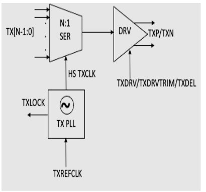
The Silicon Creations MP-PMA TX meets all the requirements for use as the electrical sub-block of a DP Source Device. Figure 4 shows a block diagram of the MP-PMA TX for DP.

Figure 4. Block Diagram of the MP-PMA TX
The salient features of the Silicon Creations MP-PMA TX include:
- Configurable serialization bus width suitable for 8b/10b or 128b/130b encoding.
- Programmable amplitude with 6 bits of control that meets the requirements of the DP standard.
- Programmable 3-tap FIR emphasis to cover the range and resolution required.
- Spread spectrum clocking generator.
- Programmable Phase-Locked Loop (PLL) BW meeting the DP specification.
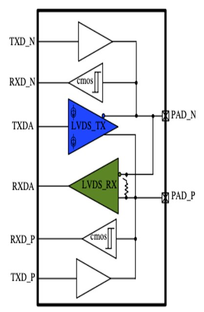
DP AUX_CH Requirements: The AUX_CH is a half-duplex AC coupled bi-directional auxiliary link that is responsible for link management. Manchester-II encoding is used for this link. The data rate is 1 Mb/s. The Silicon Creations bidirectional LVDS IO buffer can be used for the electrical sub-block of this link (Figure 5).

Figure 5. Block Diagram of LVDS AUX-CH front-end
Silicon Creations DisplayPort IP Deliverables
The Silicon Creations deliverables include a front-end (FE) kit that is composed of the LEF footprint, a Verilog behavioral model and testbench, Synopsys Liberty timing model, datasheet and application note. The back-end (BE) kit consists of the GDSII layout, Calibre LVS netlist, release notes and waivers, as well as physical verification log files. The interface to the controller is in the form of an RTL wrapper in plain text which is provided along with an application note and SDC. Silicon Creations will work with the DP controller vendor to ensure seamless integration of the Silicon Creations IP at the chip level.
Summary
DisplayPort plays an important role in many electronic products, ranging from cell phones to automobiles. Since it is based on signal and protocol technology already used in data communications, it has enabled an increase in performance and integration in audio-visual links. Silicon Creations has extensive experience developing and supporting DP and eDP Sink or Source Main-Link and AUX-Link PMA IP, offering solutions in a wide range of process nodes from 55nm down to the most advanced nodes on either flip-chip or wirebond package types.
Related Semiconductor IP
- Ultra-Low-Power LPDDR3/LPDDR2/DDR3L Combo Subsystem
- 1G BASE-T Ethernet Verification IP
- Network-on-Chip (NoC)
- Microsecond Channel (MSC/MSC-Plus) Controller
- 12-bit, 400 MSPS SAR ADC - TSMC 12nm FFC
Related Articles
- 20nm Dilemma Explained
- Combining USB Type-C and DisplayPort support in portable implementations
- Paving the way for the next generation audio codec for the True Wireless Stereo (TWS) applications - PART 1 : TWS challenges explained
- Network-on-chip (NoC) interconnect topologies explained
Latest Articles
- Extending and Accelerating Inner Product Masking with Fault Detection via Instruction Set Extension
- ioPUF+: A PUF Based on I/O Pull-Up/Down Resistors for Secret Key Generation in IoT Nodes
- In-Situ Encryption of Single-Transistor Nonvolatile Memories without Density Loss
- David vs. Goliath: Can Small Models Win Big with Agentic AI in Hardware Design?
- RoMe: Row Granularity Access Memory System for Large Language Models