Rambus Unveils PCIe 7.0 IP Portfolio for High-Performance Data Center and AI SoCs
June 12, 2024 -- The relentless innovation in Artificial Intelligence (AI) and High-Performance computing (HPC) demands a cutting-edge hardware infrastructure capable of handling unprecedented data loads. To overcome these challenges and usher in a new era of performance, Rambus is proud to announce the launch of our PCI Express® (PCIe®) 7.0 IP portfolio, encompassing a comprehensive suite of IP solutions including:
- PCIe 7.0 Controller designed to deliver the high bandwidth, low latency, and robust performance required for next-generation AI and HPC applications
- PCIe 7.0 Retimer for highly-optimized, low-latency data path for signal regeneration
- PCIe 7.0 Multi-port Switch that is physically aware to support numerous architectures
- XpressAGENTTM to enable customers to rapidly bring-up first silicon
“The burgeoning landscape of data center chip manufacturers, driven by the emergence of novel data center architectures, necessitates the availability of high-performance interface IP solutions to foster a robust and thriving ecosystem,” said Neeraj Paliwal, SVP & GM of Silicon IP at Rambus. “The Rambus PCIe 7.0 IP portfolio addresses this challenge by delivering unparalleled bandwidth, low latency, and security features. These components work together to provide a seamless, high-performance solution that meets the rigorous demands of AI and HPC applications.”
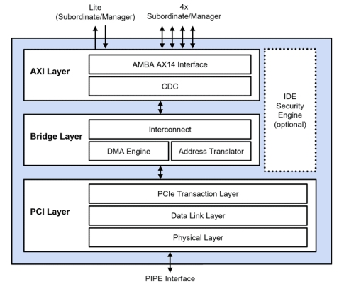
Rambus PCIe 7.0 Controller IP key features include:
- Supports PCIe 7.0 specification including 128 GT/s data rate
- Implementation of low-latency Forward Error Correction (FEC) for link robustness
- Supports fixed-sized FLITs that enable high-bandwidth efficiency
- Backward compatible to PCIe 6.0, 5.0, 4.0, etc.
- State-of-the-art security with an IDE engine
- Supports AMBA AXI interconnect

PCIe 7.0 Controller IP Block Diagram
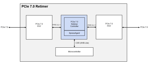
Rambus PCIe 7.0 Retimer IP key features include:
- Supports PCIe 7.0 specification x2 to x16 lanes
- Pre-integrated Xpress Agent debug analysis IP
- Highly-configurable equalization algorithms with adaptive behaviors
- Power modes and intelligent clock gating to best manage controller IP

PCIe 7.0 Retimer IP Block Diagram
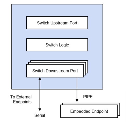
Rambus PCIe 7.0 Switch IP key features include:
- Highly scalable up to 32 ports configurable external or internal endpoints
- Physically aware to account for port placements across large die
- Superior performance through non-blocking architecture
- Allows seamless migration from FPGA prototyping design to ASIC/SoC production design with the same RTL

PCIe 7.0 Switch Block Diagram
Rambus PCIe XpressAGENT key features include:
- Non-intrusive, intelligent, in-IP debug/logic analyzer for PCIe Controller, Retimer and Switch IP enabling rapid first-silicon bring-up
- Integrates with any PIPE compliant SerDes
- Provides unified access to PHY, MAC and Link Layers locally or remotely via a CPU-agnostic API
- Provides pre-emptive monitoring and diagnosis via remote access for infield products
In addition to the PCIe IP portfolio, Rambus also offers industry-leading interface IP for HBM, CXL, GDDR, LPDDR, and MIPI. For more information, visit www.rambus.com/interface-ip.
Related Semiconductor IP
- PHY for PCIe 7.0 and CXL
- PCIe 7.0 PHY, TSMC N5 x4, North/South (vertical) poly orientation
- PCIe 7.0 PHY, TSMC N3P x4, North/South (vertical) poly orientation
- PCIe 7.0 PHY, TSMC N2P x4, North/South (vertical) poly orientation
- PCIe 7.0 PHY, TSMC Intel 18A x4, North/South (vertical) poly orientation
Related News
- Avery Design Systems and Rambus Extend Memory Model and PCIe VIP Collaboration
- Rambus Demonstrates Industry-first PCIe 5.0 Digital Controller IP for FPGAs
- Rambus Delivers PCIe 6.0 Controller for Next-Generation Data Centers
- Rambus Delivers PCIe 6.0 Interface Subsystem for High-Performance Data Center and AI SoCs
Latest News
- NEO Semiconductor Demonstrates 3D X-DRAM Proof-of-Concept, Secures Strategic Investment to Advance AI Memory
- M31 Collaborates with TSMC to Achieve Tapeout of eUSB2V2 on N2P Process, Advancing Design IP Ecosystem
- Menta’s eFPGA Technology Adopted by AIST for Cryptography and Hardware Security Programs
- Silicon Creations Celebrates 20 Years of Global Growth and Leadership in 2nm IP Solutions
- TSMC Debuts A13 Technology at 2026 North America Technology Symposium