Ultra Low Jitter Wide Band LC PLL
MoSys, Inc.
Introduction
The accelerating need for ever higher data rates and serial I/O density sets demanding performance requirements for current and next generation SerDes transceivers. Not only must they handle multiple data rates to accommodate new link speeds and standards yet retain backwards compatibility for legacy systems, but they must meet tighter performance specifications to meet the challenges of the overall link design. The PLL is the key to determining high speed link capabilities, since high quality clocks are required to meet bit error rate (BER) specifications of 10-12 to 10-15. An ultra-low jitter wideband LC PLL has been developed to meet the exacting requirements of today's systems.
High Speed Link I/O Interface Requirements
Both consumer and business trends are driving an explosive demand for system and network bandwidth at all levels from individual systems, local networks and storage all the way up to the Internet itself. YouTube, Facebook, Internet Protocol television (IPTV), smart phones, and an array of other consumer applications are the major contributors to the rapid rise in Internet traffic. The recent emergence of cloud computing for both personal and corporate applications adds to this surge in demand. As shown in Figure 1, Internet traffic is expected to quadruple between 2009 and 2014. System performance requirements come not just from the core networking infrastructure required to support Internet growth, but also from business and government demands for increasingly complex computation- and data-intensive applications such as weather prediction, financial analysis, genomics research, and design simulation. This burgeoning demand is increasingly straining systems-networks, processors, storage-and in particular the I/O linking the various elements together.

Figure 1 Growth of Internet Traffic
The next generation of high speed I/O standards for networks, computer I/O buses, and storage area networks supports these anticipated bandwidth needs with aggressive increases in performance. Current high speed transceiver data rates are typically 5 to 6 Gb/s, supporting standards such as PCIe Gen1 and Gen2, SATA-3, Optical Internetworking Forum (OIF) CEI-6G, and Interlaken. The recently ratified 40G/100G Ethernet protocol and other next generation protocols leverage 8 to 11 Gb/s transceiver rates and multi-lane architectures to achieve a total bandwidth of 100Gb/s or beyond. IEEE 802.3ba's XLAUI interface specifies four 10.3125 Gb/s lanes to achieve a bandwidth of 40 Gb/s, while CAUI's ten 10.3125 Gb/s lanes provide a bandwidth of 100 Gb/s. Interlaken, a chip-to-chip protocol based on Optical Internetworking Forum's (OIF) CEI-6G and CEI-11G electrical standards, similarly scales to 100 Gb/s. The SerDes Framer Interface (SFI) standard SFI-S, based on the same electrical standards as Interlaken, also reaches 100Gb/s to support 100G optical networks. The PCIe Gen3 computer I/O bus specification uses the somewhat slower rate of 8 Gb/s but defines x1, x2, x4, x8, x12, and x16 configurations to address the wide variety of data transfer rates required. Nor is the trend towards higher speeds slowing. Even with the migration to 40G/100G in its infancy, the industry is already anticipating 25 Gb/s transceiver rates and beyond.
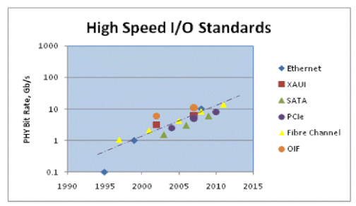
Figure 2 Higher Speed I/O Bit Rates
Circuit Design
The high performance PLL design (Figure 3) described here more than meets the challenge of today's 40G/100G multi-protocol environment. The lock frequency range of 2.3 to 5.0 GHz enables data rates from 0.6 to 10 Gb/s (with half-rate clocking). More importantly, the design maximizes tuning range and loop bandwidth while minimizing jitter across the entire operating range.
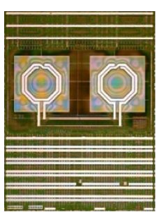
Figure 3 Micrograph of PLL
PLL Architecture
The basic architecture of the integer-N LC phase and frequency lock PLL is shown in Figure 4. Integrating programmable capacitances into the voltage-controlled oscillator (VCO) retains the low jitter of an LC oscillator based design without sacrificing the broad frequency range typical of ring oscillator based PLLs. The reference clock (REFCLK) receiver accepts a 1.8 V LVDS 156.25MHz input signal (the REFCLK frequency is selected based on the desired output frequency)
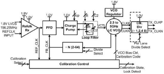
Figure 4 Integer-N LC PLL Block Diagram
and converts it to internal chip levels for the phase/frequency detection (PFD) block. The receiver is capable of operation up to 5.0 GHz to support the PLL bypass mode for debugging. The PFD output drives the charge pump and loop filter which provide the frequency fine tuning control signal VCTL to the voltage-controlled oscillator (VCO), while the coarse tuning to the nominal data rate (selectable in discrete increments tied to reference clock frequency) is set by the calibration control circuit. The integer-N feedback divider (2 to 64 in increments of 1) is custom designed for low power high frequency operation. Independent control of the data rate for each lane is possible with the per lane clock divide by I, 2, 4 or 8. Selecting divide by 8 with the PLL locked at 2.343 GHz enables 0.586 Gb/s, while divide by 1 with the PLL locked at 5 GHz enables 10 Gb/s.
Charge Pump & Loop Filter
Programmable charge pump current, loop filter resistance and ripple capacitance provide control over loop bandwidth and peaking, allowing the PLL performance to be adjusted to match the application. The charge pump current has a nominal range of 0.25 to 1 mA. A unity gain buffer from the loop filter controls the voltage across the charge pump current sources during phase detector switching. This scheme results in lower deterministic jitter and limits peaking at high bandwidth settings since it does not introduce parasitic poles into the transfer function. The loop filter output provides the fine tuning signal for the voltage-controlled oscillator.
Programmable Voltage Controlled Oscillator (VCO)
Thirty-one switchable NMOS accumulation-mode capacitors provide a wide coarse tuning range of 2.3 to 4.65 GHz, followed by fine tuning to meet the design range of 2.3 to 5.0 GHz. For any calibration code n, the fine-tuning range is sufficient to overlap the frequencies associated with codes n-1 and n+1. An on-chip regulator for the VCO supply has a bandwidth at least ten times the nominal PLL loop bandwidth. This regulator, along with the low peaking, wide bandwidth of the PLL loop, reduces the impact of power supply noise on accumulated jitter. A PMOS current source was selected because of the lower 1/ f noise compared to an NMOS implementation. The calibration circuit also sets the VCO bias current for each calibration code to maximize the output without pushing the LC oscillator into the voltage-limited region, optimizing VCO phase noise. The bias current setting is programmable to account for future process shifts. The average VCO sensitivity is fairly low, approximately 600MHz/V, to minimize deterministic jitter (DJ) and amplitude modulation to phase modulation conversion from the varactors. NMOS switching transistors feed the complementary clock signals (CLKP, CLKN) to the individual output clock dividers.
Noise Immunity
In addition to the on-chip regulator for the VCO supply and the use of PMOS current sources, several other design choices minimize noise. A separate 1.0 V analog supply is used for the PLL, while the ground is shared with the digital circuitry. Earlier research on various power supply configurations has shown this arrangement to yield the least jitter. Double guard rings shield the VCO varactors, NMOS switching transistors, digital calibration circuit, and integer-N feedback divider to improve substrate noise rejection.
Control Feature
The PLL can be readily configured for a wide variety of applications and standards. Given a REFCLK frequency, the programmable calibration code and divisor for the integer-N feedback divider set the output frequency, which is further selectable via a per lane clock divide. Loop bandwidth and peaking are also tunable through the calibration circuit. Finally, a PLL bypass option enhances system debugging capabilities.
Performance
PLL performance was characterized in silicon with the PLL embedded in an 8-lane (octal) SerDes. All measurements were taken at the output of the farthest transmitter using a clock pattern and include the effects of about one millimeter of clock distribution. A 156.25 MHz reference clock was used. The PLL delivers cutting edge performance for random jitter, bandwidth peaking, coarse tuning range and minimum hold range.
Tuning Range
To verify the PLL design range, lock was measured from 2.343 to 4.65 GHz in 156.25 MHz steps. Running the VCO open loop, the VCO frequency was measured for each calibration code and compared with simulation, as shown in Figure 5. The coarse tuning range is 67%, with a minimum hold range of 9.6% (226 MHz at 2.3 GHz) and a maximum hold range of 17.2% (800 MHz at 4.65 GHz). The frequency spectrum of the PLL locked at 5 GHz, with reference clock spurs at -50.81 dB, is shown in Figure 6.
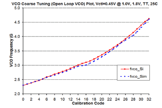
Figure 5 VCO Coarse Tuning Plot
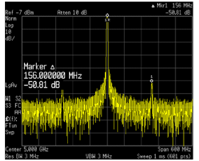
Figure 6 Frequency Spectrum for PLL Locked at 5GH
The measured lock time is 32 micro seconds at 3.125 GHz and 58 micro seconds at 5 GHz.
Phase Noise & Output Jitter
Output jitter and closed loop phase noise were characterized and the PLL was found to exhibit excellent performance as targeted in the design. The closed loop phase noise at 1 MHz offset is -117.18 dBc/Hz at 3.125 GHz and -109.31 dBc/Hz at 5 GHz, as shown in Figure 7. Jitter performance is comparable to the best results published to date, with RJrms measured to be 548 fs at 3.125 GHz and 460 fs at 5 GHz.
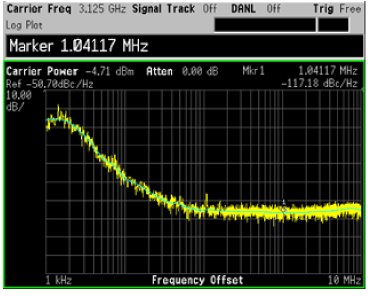
Figure 7 PLL Phase Noise at 3.125GHz
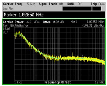
Figure 8 PLL Phase Noise at 5.0 GHz
Total jitter at these frequencies is 13.83 ps and 11.41 ps respectively. Jitter measurement results for a clock pattern at the Tx are shown in Figure 9 for 6.25 Gb/s and in Figure 10 for 10 Gb/s, and in Figure 11 and Figure 12 for a PRBS11 pattern, respectively. These results easily meet the jitter specifications for 10G Ethernet and other multi-gigabit standards. Eye diagrams for a PRBS11 pattern are shown in Figure 10.
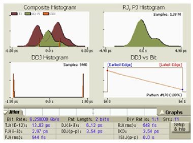
Figure 9 PLL plus Transmit (TX) Jitter for Clock Pattern at 6.25Gbps

Figure 10 PLL plus Transmit (TX) Jitter for Clock Pattern at 10.0 Gbps
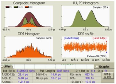
Figure 11 PLL plus Transmit Jitter for PRBS-11 Pattern (6.25 Gbps)
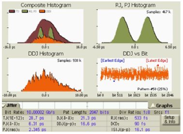
Figure 12 PLL plus Transmit Jitter for PRBS-11 Pattern (10.0 Gbps)
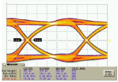
Figure 13 Transmit (TX) Eye Diagrams for PRBS-11 at 6.25Gbps
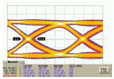
Figure 14 Transmit (TX) Eye Diagrams for PRBS-11 at 10.0 Gbps
Loop Bandwidth
The PLL bandwidth and peaking are programmable from 1.5 to 10 MHz across the VCO frequency range with a maximum peaking of 1.6 dB. Figure 10 shows the closed loop transfer function at 3.125 GHz with a measured loop bandwidth of 9.74 MHz and peaking of 0.81 dB. Measured results correlate well with the values derived from the PLL model using capacitances back-annotated from layout.
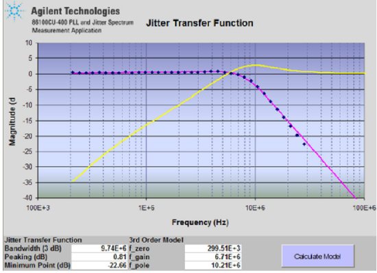
Figure 15 Jitter Transfer Plot at 3.125 GHz with Maximum Loop Bandwidth Setting
Power & Area
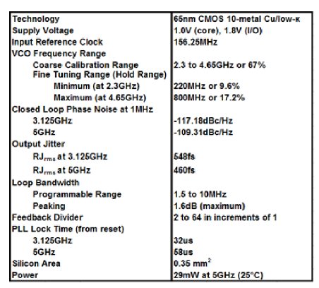
PLL power consumption is 25 mW at 5 GHz (nominal supply voltages and room temperature). With an area of 0.35mm2, the PLL provides superior performance at a small area penalty compared to ring oscillator based designs. Table 1 summarizes the measured performance.
Table 1 PLL MeasuredPerformance Conclusion
The silicon results demonstrate that the programmable loop filter and wideband VCO architecture presented here is clearly competitive with other PLL architectures for multigigabit applications. The design advantages include very low jitter without sacrificing a wide tuning range, a wide loop bandwidth with peaking limited to a maximum of 1.6 dB, and low power consumption. The PLL is compatible with a variety of multi-gigabit/s wireline standards such as SONET OC-192, PCIe (Gen1, Gen2, and Gen3), 10GBASE (-CX4, -KX4), 1000BASE-X (SGMII), SFI-S, XFI, Interlaken, XLAUI, and SRIO. It is compliant with the PCIe Gen2 and Gen3 loop bandwidth specifications, and for Gen2 provides the option to run the PLL locked at 2.5 GHz with an output clock divide of 1 or at 5 GHz with an output clock divide of 2.
Related Semiconductor IP
Related Articles
- Ultra Low Power Designs Using Asynchronous Design Techniques (Welcome to the World Without Clocks)
- Mixed Signal Drivers for Ultra Low Power and Very High Power Applications
- A 55-nm Ultra Low Leakage SRAM Compiler with Optimized Power Gating Design
- Implementing Ultra Low Latency Data Center Services with Programmable Logic
Latest Articles
- Enabling RISC-V Vector Code Generation in MLIR through Custom xDSL Lowerings
- A Scalable Open-Source QEC System with Sub-Microsecond Decoding-Feedback Latency
- SNAP-V: A RISC-V SoC with Configurable Neuromorphic Acceleration for Small-Scale Spiking Neural Networks
- An FPGA Implementation of Displacement Vector Search for Intra Pattern Copy in JPEG XS
- A Persistent-State Dataflow Accelerator for Memory-Bound Linear Attention Decode on FPGA