Reusable Verification Infrastructure for A Processor Platform to deliver fast SOC development
by Kambiz Khalilian, Stephen Brain, Richard Tuck, Glenn Farrall
Infineon Technologies
Abstract:
This paper describes a platform developed at Infineon for the efficient re-use of IP for SOC design. Use of a pre-configured and pre-verified suite of code means that adaptation and subsequent re-verification of the code for specific applications is greatly eased.
1. The Generic Platform:
The TriCore Integration Platform (TIP) is an SOC development platform based on the TriCore microprocessor for rapid application- and system development. It is integrated into a complete chip reference design and a chip level test bench, which runs “out-of-the-box”. The reference chip shortens customers time-to-market and allows the rapid development of derivatives. The platform includes the configurable TriCore microprocessor core, and required system- and general-purpose peripherals. Standard bus ports are provided for the addition of user peripherals. The deliverables include hardware and software components as well as tools and a verification environment, which supports the customization and configurability of the platform.
2. Configurability:
Most embedded applications are cost sensitive and require customized solutions. Some applications require a large amount of on-chip memory, others require a high-bandwidth interconnect to off-chip resources. Some applications require a high-performance computing engine; others need to satisfy low-power requirements of mobile- and handheld devices. Each application has specific requirements, which needs to be considered in the design of a generic platform. Unfortunately there is no “one size fits all” platform that can satisfy all these requirements. Therefore a generic platform, which is the basis for the development of multiple applications and derivatives, needs to be highly configurable. The configuration needs to be at two levels, firstly at module level where issues such as memory size are determined and then at system level where the number and type of peripherals is defined.
Some configurability is performed at RTL and synthesis level and modules will be enabled or removed by the designer during the chip development cycle. Additionally some configurability remains at board level, which gives application engineers the required flexibility to optimize and fine-tune the system. The software engineer can achieve the last instance of configurability via the instruction set of the processor to set up various functions such as configuring the GPIO, as inputs or outputs; switching-on or off the MMU or caches and configuring the external bus memory configuration.
3. The Configurable TriCore Microprocessor System:
• Architecture:
TriCore is a single-core 32-bit MCU-DSP architecture optimized for real-time embedded systems. TriCore architecture unifies the best of three worlds – real-time capabilities of microcontrollers, computational prowess of DSPs, and the highest performance/price implementations of RISC load-store architectures. The TriCore architecture is implemented as a family of cores that offer tremendous scalability in terms of both price and performance.
• TriCore Benefits and Features
The TriCore Microprocessor System (MPS):Benefits:
• Integrated MCU-DSP instructions in one core
• Fast and efficient processing of multiple tasks on one engine
• Low code size and inherent high level language support
• One development toolset for both MCU and DSP tasks
• Higher flexibility and lower costFeatures:
• 32-bit load-store Harvard architecture
• SuperScalar execution
• 16 address and 16 data registers
• Fast Context switch & low interrupt latency
• 16-bit and 32-bit instruction formats
• Powerful bit manipulation support
• Sustained throughput of two 16x16 MACs per clock
• SIMD packed arithmetic and zero overhead loops
• DSP addressing modes and saturated math
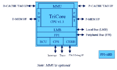
The TriCore Microprocessor System (MPS) consists of the TriCore CPU, with dedicated interfaces for program and data, an optional memory management unit (MMU), optional cache tags for data and program and a system support unit (SSU). The CPU memory interfaces support up to 16K cache and up to 64K tightly coupled memories for program and data. The SSU integrates the Debug and Trace Unit, the Interrupt Control Unit, a local memory bus hub (LMBH), and the FPI bus bridge for connecting system- and application-specific peripherals.
The TriCore Integration Platform has been designed in such manner that allows users to configure the platform at all levels of abstraction. The IC development team can use the “out-of-the-box” configuration or fine-tune the platform for best cost-performance ratio. For example, the IC designer is able to add an optional MMU or a Co-Processor to the TriCore CPU, specify the size of the tightly coupled memories for program- and data, or add caches of different sizes to the processors memory subsystem. Some of the configurability, which can be achieved at RTL and synthesis level, is listed below:
• Optional MMU
• Optional Cache
• Optional Co-Processor (COP), i.e. FPU
• Size of tightly coupled program- and data- memory
• Size of program- and data- Cache
• Support of multi-layer bus infrastructure: bus interface and bridges
• Number and priority of masters accessing the peripheral bus
• Priority of masters in test and debug mode
• Addition and removal of platform peripherals

Additionally many of the system- and platform peripherals are also configurable via generics and parameters. The delivered EDA scripts allow users to configure the features at RTL and synthesis level.
The configurability and the complexity of the design parameters provide a real challenge to the verification environment as not only must a standard set of tests and a test bench be delivered with the product but verification of the derivatives must also be supported without extensive modifications of the verification suite.
4. Platform features:
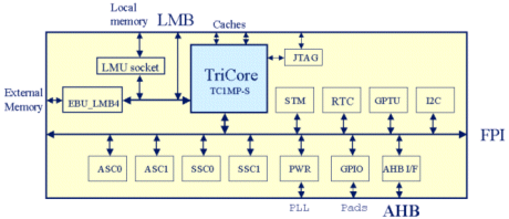
- TriCore Microprocessor System:
- TriCore CPU
- Optional MMU
- Optional COP/FPU
- Tightly Coupled Program and Data Memory
- Interrupt Control Unit (ICU):
- Programmable, up to 255 levels; 255 priorities
- Debug & Trace Unit:
- System access via JTAG port and CPU trace
- System Control Unit (SCU):
- Watch Dog Timer
- Reset Control Unit
- Power Manager
- LMBH:
- Local Memory Bus Hub for the Processors 64-bit Local Bus.
- EBU:
- External Bus Unit, for off-chip peripheral and memory access.
- BCU:
- Bus Control Unit for the FPI peripheral bus.
- ASC:
- Asynchron/Synchron Control
- SSC:
- Serial Synchron Control (SPI compatible)
- STM:
- System Timer
- RTC:
- Real-Time Clock
- GPTU:
- 3x 32-bit General Purpose Timer Unit
- GPIO:
- General Purpose I/O
- I2C:
- 2 Channel I2C Serial Bus
- AHB Bus Bridge.
5. The Reference Chip:
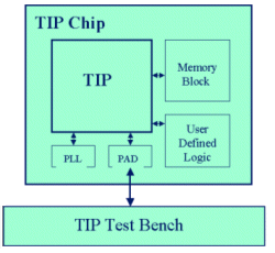
The platform is integrated into a complete chip reference model. A chip level test bench surrounds the chip reference model. On-chip resources are accessed through the pads. The reference chip runs “out-of-the-box” with the provided test bench. This allows customers to run simulations and evaluate the platform. Once the required confidence level has been achieved customers can configure the platform to their needs and add application-specific logic to the provided interfaces.
The platform itself is provided in synthesizable RTL and can be easily ported to new technologies and process. The reference chip, which integrates the platform, includes other components, which are required to build a complete SOC such as memory models, PLL and pads. In order to provide a working reference design these are provided as generic models, but for fabrication the memories and the PLL are foundry specific and final versions would be provided from the silicon vendor.
In addition all interfaces, which are required to build a customized SOC are provided in a template (UDL= User Defined Logic). Customers will add the application-specific logic to the provided bus and interrupt infrastructure.
6. The platform deliverables:
According to Sangiovanni-Vincetelli, a key originator of the platform concept, a platform can be categorized in 2 abstraction layers. The upper layer allows software designers to develop applications without referring to the lower levels of abstraction. The lower view is a set of rules that classify a set of components belonging to the platform.

The TriCore SOC Platform is a complete reference design, which allows designers to knock-off derivatives of their SOC in a very short cycle. Therefore the deliverables cover both abstraction layers.
The platform deliverables include:
• RTL model for Platform and Reference Chip, Test Bench, and EDA Scripts
• Bus Functional Models & Protocol Checkers
• Firmware, Peripheral Software Configuration Tool
• GNU C/C++ Compiler, Assembler, Debugger, Linker
• Cycle Accurate Instruction Set Simulators
• DSP Libraries
• OS-kit
• Java Acceleration Support
• FPGA Prototyping Boards

7. The EDA Design flow
The design flow consists of the following steps:
8- The Verification Environment
- Configure Platform - e.g.. define size of caches, memory size, number of peripherals.
- Add Application-Specific Logic.
- Simulate and verify RTL.
- Replace Foundry-Specific Models (if applicable) - TIP supplies generic models which the designer will replace using the foundry specific library modules.
- Simulation
- FPGA prototyping - an FPGA prototyping facility is available with TIP.
- Chip Synthesis.
- Layout/FloorPlan.
- STA and gate level simulation -here the designer can rerun many of the verification tests supplied with the RTL.
- Tape-out.
Flow and Tools
In developing a testbench and verification methodology, a key assumption has to be that it must support the typical environment seen in the majority of users. Although there is increasing use of verification techniques involving formal methods or random test generation they are not yet at the point where it can be assumed that every potential user has access to these.
One advantage of providing a preconfigured and preverified platform however is that the verification at Infineon can be performed using these tools and techniques, as once verified, the bulk of the code is not going to change and therefore does not need further verification.

In view of this, the tool flow for the end user is fairly simplistic, only an industry standard simulator and TriCore assembler tools being required. The testbench is provided with scripts for assembling code and loading the memory images etc and these can be modified as required by the user.
Infineon has a proprietary design flow called Inway. This is a design environment used across the company and allows interchangeability and reuse of IP across sites. The TriCore Platform was developed using Inway and then exported into a non-Inway environment. As each user will have different ideas about design structure, file organization, environment variable setup etc it is impossible to have a one size fits all flow. Therefore it was decided that the non-Inway exported platform would bear a strong resemblance to Inway in its organization and users will either map it “as is” into their design environment or change it to fit exactly.
Methodology
A verification methodology for an SOC design or a microprocessor-based system will often include removal of the microprocessor and verification of the remaining busses and peripherals using some form of BFM (bus functional model). Once these have been verified, the processor is reinserted and further testing carried out using the cpu. Tests are written in assembler or C.
For a configurable platform such as TIP much of this is not necessary. Many designers and verification engineers see BFMs as unnecessarily intrusive and complex as they have to be inserted for verification at RTL and then removed again later prior to synthesis. As TIP is supplied pre-verified the busses and peripheral blocks are already guaranteed functional and user verification of these in isolation to he cpu is not necessary. This means that further verification can concentrate on the value-added portions of the design – i.e. those parts which have had some modifications such as configuration or removal of peripherals or where modules have been added.
Verification
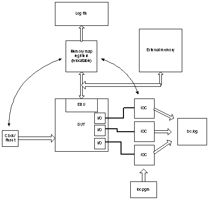
For this verification, self-checking directed tests using the CPU are highly effective. The keys to this are to ensure the test bench has the appropriate support for generating and checking data on the peripherals and that there are powerful macros supplied with the assembler sufficient to raise the level of abstraction of tests to an extent where they can be quickly and reliably written.
For example, on TriCore it takes 2 instructions to form a 32-bit address word and 2 more to generate a 32-bit data word so to write a 32 bit data word to a peripheral would take several instructions. As this is a common operation, a single macro can easily replace it.
Of course, this is a trivial example, but it does demonstrate that judicial use of macros can greatly assist the creation of verification tests by raising the abstraction level and without the added complexities of requiring high level language support.
With the TIP platform are supplied a set of verification tests to demonstrate the following:
• Sign of life. To check that the installation has been done correctly, that it functions in the user’s environment and that there is a working toolchain.
• Integration tests of modules that can be modified removed or changed by the user. The tests themselves are configurable so that for example if a peripheral’s connectivity or address changes, the test program adapts automatically. Also if a peripheral is removed, then the test is automatically removed from the regression list.
TIP
The TIP block diagram shows a number of busses. There are two internal, proprietary busses, which are used for Infineon-supplied peripherals and internal memory traffic. As all this is standard IP, which has been re-used many times, basic integration tests are sufficient to ensure functionality.
An AHB interface is also supplied as it is expected that many designers will want to add their own (or bought in) IP via this interface. This has the benefit of being an industry standard with an extensive knowledge base of not only IP but also engineering expertise on how to use it.
Verification of this takes place mainly through conformance testing against the AHB interface specification. There are compliance checkers commercially available and within Infineon these are applied to the bridge in order to check compliance.
All the above refers to platform level verification. Clearly the end product is expected to be an SOC and the advantage of an approach such as the one just described is that many, if not all, the tests can be applied at gate level after synthesis. The prime requirement of the platform is to support the rapid design and verification of RTL, but there is nothing implicit in the package to prevent it being used in other phases of the flow.
9. Summary and Conclusion
The TriCore Integration Platform allows designers to concentrate on the value-added parts of their design by using a pre-configured and pre-verified platform. Future work allows application specific versions of the platform to be developed for particular market segments.
10. Authors
Kambiz Khalilian, Infineon Technologies NA Corp., San Jose, CAStephen Brain, Infineon Technologies UK Ltd, Bristol, UK
Glenn Farrall, Infineon Technologies UK Ltd, Bristol, UK
Richard Tuck, Infineon Technologies UK Ltd, Bristol, UK
Related Semiconductor IP
- ReRAM NVM in DB HiTek 130nm BCD
- UFS 5.0 Host Controller IP
- PDM Receiver/PDM-to-PCM Converter
- Voltage and Temperature Sensor with integrated ADC - GlobalFoundries® 22FDX®
- 8MHz / 40MHz Pierce Oscillator - X-FAB XT018-0.18µm
Related Articles
- A RISC-V Multicore and GPU SoC Platform with a Qualifiable Software Stack for Safety Critical Systems
- Early Interactive Short Isolation for Faster SoC Verification
- FastPath: A Hybrid Approach for Efficient Hardware Security Verification
- A Generic Solution to GPIO verification
Latest Articles
- SoK: From Silicon to Netlist and Beyond Two Decades of Hardware Reverse Engineering Research
- An FPGA-Based SoC Architecture with a RISC-V Controller for Energy-Efficient Temporal-Coding Spiking Neural Networks
- Enabling RISC-V Vector Code Generation in MLIR through Custom xDSL Lowerings
- A Scalable Open-Source QEC System with Sub-Microsecond Decoding-Feedback Latency
- SNAP-V: A RISC-V SoC with Configurable Neuromorphic Acceleration for Small-Scale Spiking Neural Networks