Challenges in PCI Express IP Implementation
Prakash Bare, Rambus, Inc. - Los Altos USA
J.Balachandran, IMEC. - Belgium
Abstract:
With the advent of high-speed point-to-point serial interconnect standards like PCI Express, data transfer rates have improved dramatically by several orders of magnitude. For example, PCI Express can provide sustained data transfer rates of 250 MB/s and higher. As a result, several market segments including next generation computing and communication SOC platforms have started deploying PCI Express technology. While there is tremendous momentum for great market adoption, PCI Express also poses significant challenges to the design community. Availability of high quality PCI Express IPs has helped address some challenges to a certain extent. Nevertheless, IP selection, verification and integration are key aspects to the success of an IP-based design. This paper describes some of the challenges imposed by an IP based implementation of the technology and discusses about possible solutions to address them.
INTRODUCTION
PCI Express is a serial point-to-point interconnect standard, capable of driving data at speeds greater than 250 MB/s. In addition to the high speed and limited pin count, its backward compatibility with legacy standards such as PCI and PCI-X have been major factors in driving the market adoption. PCI Express offers a wide range of options to choose from, in order to cater to multiple market segments. Furthermore, advanced error reporting and interrupt capabilities enable improved reliability, availability and serviceability of PCI Express based systems. While these are just a few advantages of the technology, the configurability and complexity of PCI Express pose several challenges to the designer. The designer needs to read and understand several huge specifications associated with the standard in order to be able to select the options that need to be incorporated in the design. Some of the configurable features include the following:
- Link width from x1 to x32
- Endpoint, Root complex or Switch
- Maximum packet size – 128 bytes to 4 KB
- Number of functions – 1 to 8
- Number of Virtual Channels – 1 to 8
- Error reporting
- Interrupt support – INTx/MSI/MSIX
It must be noted that design and verification complexity exponentially increases with such a huge sample space of configurable features. A minor error in judgment while selecting the configuration can make the design unsuited for the targeted application and prolong the time to market. Moreover, the right configuration will help in optimizing the cost for the application along with optimal power, performance and area.
The above factors coupled with a dearth of domain expertise and huge verification effort required make PCI Express, a strong candidate for third party IP-based design. Some IP vendors provide tools that can be used to pick the optimum configuration for an application. These tools will guide the designer and simplify the process and reduce the number of iterations required in selecting a configuration. The rest of the paper focuses on IP-based PCI Express implementation
DYNAMIC CONFIGURABILITY OF IP
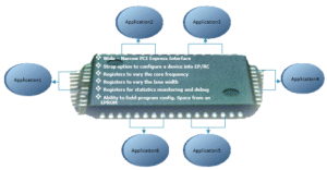
An IP can provide several dynamically configurable options that can be used to improve market reach. As shown in Figure 1, by programming a few registers in the IP, the chip can be utilized for more than one application scenarios. For example, the same design can be used as an Endpoint or a Root complex device through a strap option provided in the IP.
Figure 1. Dynamic configurability to improve market reach
Register interfaces for debugging and performance monitoring will add value to the design. These are especially useful during post-silicon validation phase and for performance or power analysis.
IP COMPLETENESS AND SUPPORT
It is not sufficient for a design IP to be just compliant to the PCI Express specification. It is equally critical for the design IP to be complete in all respects of the specifications. A design could claim compliance and interoperability by implementing only the basic bare-essential features. In order to fully utilize the technology, advanced features have to be implemented with all the options.
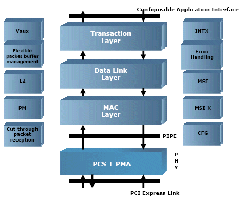
For example, a PCI Express IP could be still functional by implementing the basic blocks like Transaction, Data Link and MAC layers. However, if the design does not support advanced error reporting, it is not suitable for segments like server market. Another example could be lack of comprehensive support for power management features, which are crucial for low-power market segments. Design IPs missing key features like Vaux/L2, MSI-X or even the PCS layer are not uncommon. One of the major grey areas in a design IP is the implementation of the transaction layer. A flexible and complete transaction layer is critical for the target application and overall performance of the SOC
Missing functionality and features in design IP imposes additional burden on the consumer in terms of design, integration and verification effort. This has a direct impact on time-to-market and increases risk. An example of a feature-rich PCI Express design IP is shown in Figure 2.
A complete design IP by itself is not a sufficient criterion for the success of the project. The extent of support provided by the IP vendor must play a key role during the IP selection process. Well coordinated and expert support is required across almost every phase of the design cycle starting from architecture modeling and integration through verification, validation and interoperability testing.
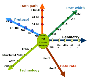
Another important aspect in IP support is the roadmap of the IP vendor. IP vendor must be committed to next generation enhancements in order to migrate to future PCI-Express based designs in a smooth manner. For example,

Figure 2. Example Feature-rich PCI Express IP

Figure 3. Broad PCI Express Portfolio
VERIFICATION CHALLENGES
The need for excellent domain expertise to accurately interpret the PCI Express specification makes the verification problem harder. In addition to the several thousands of PCI-SIG compliance check list items, there will be an equal number of design specific and corner cases that need to be covered. One way to alleviate the problem is to ensure that the design IP provides 100% SIG checklist coverage and passes all SIG compliance tests on an FPGA or an ASIC test chip. It is also important that the IP vendor participates actively in interoperability and compliance forms focusing on PCI Express.
The block level compliance tests provided by the design and verification IP vendors must be leveraged to reduce the effort. The Verification IP’s vendor specific coverage monitors will also help. A close partnership between the design IP vendor and multiple Verification and PHY IP vendors will help address the problem to a large extent. It must also be noted that a configurable test bench environment is necessary in order to suit multiple applications and interfaces. Several innovative verification methodologies and expertise including formal concepts are added values that an IP vendor can offer.
PERFORMANCE AND AREA CONSIDERATIONS
In addition to functional verification, performance should be a key aspect of the verification effort.
Link utilization, bandwidth and packet round-trip latency contribute significantly towards improving performance. Low link utilization and large latencies mitigate the advantages of deploying high-speed interconnects like PCI Express.
It is very important to include performance analysis in the early stages of the design cycle to avoid re-spins due to performance issues. Several factors including buffer sizes, flow control credit release latency and packet size affect performance.
Large buffer and packet sizes improve effective link utilization while a fast scheduler can reduce flow control credit update latencies. However, it is not feasible to implement infinitely large buffers as that will dramatically increase gate count.
In addition, area depends on several factors including the number of virtual channels supported in the configuration, maximum packet size, data path width, link width and number of functions.
Hence, it is necessary to perform thorough performance and area analysis before selecting a configuration and architecture.
IP INTEGRATION
Integration of the IP with the target application can be very time-consuming and error-prone. As mentioned earlier, the design IP needs to be highly configurable in order to suit the needs of the application. Any mismatch will result in loss of time and money. Even if the interface is suitable for the application, it must be easy to understand and use.
This will significantly reduce the effort required by the consumer during integration. Additionally, an interface which facilitates low latency, high performance packet transfer is highly desirable as it contributes in boosting overall system performance.
It must also be equally straightforward to integrate the Design IP with the Verification IP. To achieve this, the VIP must be highly portable with support for multiple modern verification methodologies.
A VIP with proven integration and support will enable verification engineers to focus on design bugs rather than debugging test bench issues.
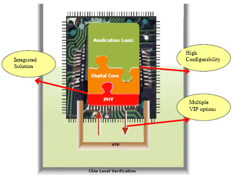
Furthermore, integrating the digital and PHY IPs can be challenging. Quality of the PHY is extremely critical to project success as it directly affects the post-silicon bring-up. An IP solution with proven, interoperable digital and PHY cores bundled together will be able to resolve the problem. An integrated solution from a single vendor may also help in reducing licensing time and cost.

Figure 4. IP Integration challenges
SUMMARY
Although PCI Express holds a lot of promise in terms of performance and functionality, the associated implementation complexity and challenges can be daunting to designers and verification engineers. This paper described some key factors which make PCI Express better suited for IP-based implementations. The IP selection, integration, support, verification and interoperability are significant challenges imposed on the design community. With careful IP selection, it can be extremely beneficial for better time-to-market and cost. A well-defined approach to each phase of the design cycle is required to address the challenges.
REFERENCES
1. PCI Express Base Specification Revision 1.0a and 1.1, PCI SIG
Related Semiconductor IP
- Configurable PCI Express 4.0 Link Controller
- PCI Express PHY
- Multi-Channel Flex DMA IP Core for PCI Express
- PCIe - PCI Express Controller
- PCI Express PIPE PHY Transceiver
Related Articles
- A low-cost solution for FPGA-based PCI Express implementation
- Challenges in verifying PCI Express in complex SoCs
- Integrating VESA DSC and MIPI DSI in a System-on-Chip (SoC): Addressing Design Challenges and Leveraging Arasan IP Portfolio
- How HyperTransport and PCI Express complement each other
Latest Articles
- An FPGA-Based SoC Architecture with a RISC-V Controller for Energy-Efficient Temporal-Coding Spiking Neural Networks
- Enabling RISC-V Vector Code Generation in MLIR through Custom xDSL Lowerings
- A Scalable Open-Source QEC System with Sub-Microsecond Decoding-Feedback Latency
- SNAP-V: A RISC-V SoC with Configurable Neuromorphic Acceleration for Small-Scale Spiking Neural Networks
- An FPGA Implementation of Displacement Vector Search for Intra Pattern Copy in JPEG XS
