A Novel Methodology to Design and Verify companion SoCs in a single package
Freescale Semiconductor India Pvt. Ltd.
Introduction
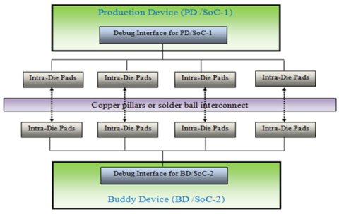
With growing complexity of System-on-Chips (SoCs), functional debug of the additional hardware becomes a greater challenge. There may be multiple SoCs with common interface present in the same package. With evolution of these complex architecture, need arises not only for design innovation but also for verification strategy which can help verify such design quickly and effectively. This paper discuss about the need to have such design and its efficient verification methodology. In these designs we are trying to enhance the debug capabilities of one SoC (says SoC-1) by using the debug support of another SoC (say SoC-2). The two SoCs are connected to each other via copper pillars and are bonded together in the same chip package. These SoCs are interacting with each other using Debug and Calibration Interfaces (DCI) provided on both the SoCs.

Figure 1 Design Architecture
Design Aspect
The impetus towards this methodology is to achieve silicon die saving which will not only reduce the cost of the chip but also its size. Production Device, SoC-1(SoC whose debug capabilities are getting enhanced), will go for final production. Its companion device SoC-2 has larger overlay memory (for storing trace/debug data) and a high speed debug interface for application debugging purpose. Since advanced debug capabilities are required by customer during initial phase of application development, this can be catered by combining the capabilities of both SoC-1 and SoC-2 together and in the final phase, only SoC1 can be sufficient. In this way additional silicon required for debug features in SoC-1 is reduced and at the same time a high speed interface with larger overlay memory is present for application development. SoC-1 can also be called as the P-Device/PD and SoC-2 as the C-Device/CD. The combination of the two is referred to as Emulation Device or E-Device/ED.
Design Requirements
High speed interface:
A high speed DCI present on C-Device can be used for debugging purpose at customer end. This high speed interface is required for faster debug capabilities at initial phase of application bring up. But once application has matured a slow interface present in PD can suffice for production.
Large overlay memory:
A large overlay memory in C-Device can be used to store the debug data during initial phase of application bring up which is not required once application gets calibrated and matured. So by not using such large memory in P-Device, significant silicon saving is achieved.
Top-On-Topology:
Both P-Device and C-Device dies are connected through copper pillars with later sitting on former further saving the package cost per SoC .
Complete isolation:
The most important feature is the supply and power regulation. This architecture demands individual supplies for the CD and the PD. Power Regulation Units (PRU) are used to help us identify the presence of CD along with PD or PD standalone. Another important feature of this design architecture is to make sure proper isolations are present to avoid leakage currents when one of SoC is switched off and the other is switched on. This can be done by having proper isolation cells in place. Isolation is needed when one of the SoC is powered-off hence based on supply information Power Regulation Unit can be enabled or disabled for the SoCs. For e.g. if C-Device is OFF P-Device regulator will detect status of C-Device and assert isolation from C-Device and vice-versa .This helps in reduction of static power leakage.
Reset phase synchronization:
For ED to work properly there is a mandatory requirement for both CD and PD to work in synchronization. Since CD is a companion device which will be assisting the PD so reset sequence of CD must not affect PD but CD must be aware of reset phases of PD for synchronization purposes.
Testing requirement:
Since ED and PD are functionally equivalent so it is mandatory that PD can be tested from ED interface as well.
Debug/Trace Message Routing (TMR):
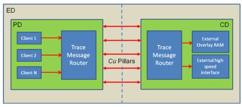
Trace message data routing is very important feature of design where debug/trace data from PD can be routed towards CD through copper pillars. This data is further routed inside CD. PD clients will send the data to the PD TMR which acts as the only client of the CD TMR. Hence any client can be directly accessed through CD TMR and data can be stored in either CD’s larger overlay memory or can be passed on to high speed external debugger.

Figure 2: Trace Message Routing
Verification Aspect
The methodology explained, is to verify multiple SoCs in a single verification environment. This is very useful especially in Power-Train segment SoCs which usually demands greater debugging and calibration needs. Now this is achieved using an additional SoC (CD) to enhance the debug capabilities and calibration support to the main SoC (PD).
Both PD and CD can be verified independently in separate verification environments but since customer is going to use both as one package(ED) so ED’s verification aspect includes:
- Verifying interconnects between PD and CD inside ED top.
- One SoC feature can be controlled through other (e.g. test mode entry)
- Timing critical paths (interfaces)
- Booting and power sequencing
- Isolation when one of the SoC is powered down.
Verification Approach
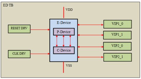
Both these SoCs (PD and CD) are instantiated in a top level device called the E-Device(ED) in the verification testbench. The ED is a topmost level module created to instantiate the SoCs and connects all the SoC-1(/2) to SoC-2(/1) signals. These signals are further connected in the SoC-1(PD) and SoC-2(CD) top modules for further connectivity within the SoCs
The main objective was to develop a modular approach for testbench so that PD (SoC-1) stimulus could be reused in ED testbench environment. The ED testbench is nothing but an augmented version of the PD testbench incorporating the CD testbench as well.
Need for testbench to cater multiple SoCs
Following things were taken into consideration while bringing up the ED testbench
- Since the E-Device(ED) will be used for development (which involves customer application debug) and the Production Device (PD) for the product (final product at the customer’s hand), they must be functionally equivalent to guarantee that the developed application will run exactly in the same way.
- Both PD and CD SoC verification use VIPs to reproduce the behavior of each other when verified standalone. This can mask timing problems between the SoCs. To solve this all the connections between the SoCs (PD and CD) are checked and verified without the use of such VIPs
- All differences between PD and ED are debug-related so all the debug tests are run from the debugging module (CD) side that must have full control over the PD SoC (supply, reset, boot).
Testbench Development Flow
The development of the testbench started by removing the VIPs connected with the copper pillars and including the same instances as used in the CD testbench into ED testbench. The modifications included the hierarchy changes as another top level (ED) has been created, updating the testbench classes, drivers, etc. and inclusion of the new ED specific VIPs. The figures 3, 4 and 5 explain the concepts.

Figure 3 Testbench Architecture of P-Device

Figure 4 Testbench Architecture of C-Device
Both CD and PD have separate monitors, drivers, and checkers along with their reset driver. But in ED, a single reset driver was created. In ED, each monitor and driver has to be enabled or disabled based upon which device is ON. And if both are working together (in debug and calibration cases) every driver and monitor becomes active. This was again controlled with the help of PRU unit.

Figure 5 Testbench Architecture of E-Device
Challenges and Solutions:
1. Huge runtime:
Since multiple SoCs in the ED testbench environment becomes a complex design, simulation time is significantly increased.
Solution: Incremental elaboration and single snapshot flow was used to reduce the simulation time.
2. Stimulus reuse:
Since both ED and PD should be functionally equivalent except from debug capability point of view so stimulus has to reused across both. But since hierarchies are different so hierarchy changes need to be carried out.
Solution: ‘defines’ based approach was used. So all the hierarchy changes were controlled through the single topmost ‘define’ file and this file can be easily ported.
3. VIP reuse:
VIPs which are used for PD or CD verification need to be reused at ED level
Solution: Sequences, drivers and monitor are coded with ‘defines’ which can be easily changed as environment changes from PD to ED.
4. Power connectivity and isolation check:
Both PD or CD can be switched ON/OFF independent of each other so isolation between the two needs to be checked properly.
Solution: Power aware simulations were carried out to verify.
Benefits:
1. Reusability:
This is one of the major advantages of this approach. The main reason for developing a single testbench is reusability. In ED complete testbench of the PD and CD can be reused. Stimulus from the CD and the PD SoC verification could be used to verify PD-CD interconnections with minimum updates.
Presently both the SoCs are verified individually in their separate testbench. Both the testbench use the same VIP versions and the effort to integrate the entire CD testbench was low and easier to execute without causing any modifications in the CD SoC verification.
2. Silicon / Cost saving:
During production phase, only PD will be manufactured as most of customer application debug has happened through ED. So, this will not only reduce the cost of silicon but also other associated cost like Production Engineering, packaging cost which would have been higher if we had provided all the CD functionality in the PD itself.
3. Debug and Calibration enhancement:
Customer can use ED for calibrating and debugging its application because it has faster debug interface in addition to large overlay memories to store trace and calibration data. Once application has become stable fewer debug capabilities are sufficient and hence PD alone can be used.
Authors:
Nitin Goel: Done B.E. in Electronics and Communication from Netaji Subhash Institute of Technology in 2006, 6+ year of industry Experience in SoC IP and Core Verification, right now working as Senior Design Engineer with Freescale Semiconductor
Amitav Halder: Done B.Tech. in Electronics and Communication from MITS Gwalior in 2004 , 9+ year of Industry Experience in SoC , IP Verification , Right now working as Lead Verification Engineer with Freescale Semiconductor
Aashish Sharma: Done B.E. in Electronics and Communication from Delhi College of Engineering in 2012, 1+ year of experience in SoC verification, right now working as Design Engineer with Freescale Semiconductor
Related Semiconductor IP
- Ultra-Low-Power LPDDR3/LPDDR2/DDR3L Combo Subsystem
- 1G BASE-T Ethernet Verification IP
- Network-on-Chip (NoC)
- Microsecond Channel (MSC/MSC-Plus) Controller
- 12-bit, 400 MSPS SAR ADC - TSMC 12nm FFC
Related Articles
- Integrating VESA DSC and MIPI DSI in a System-on-Chip (SoC): Addressing Design Challenges and Leveraging Arasan IP Portfolio
- It's Just a Jump to the Left, Right? Shift Left in IC Design Enablement
- BCD Technology: A Unified Approach to Analog, Digital, and Power Design
- VLSI Physical Design Methodology for ASIC Development with a Flavor of IP Hardening
Latest Articles
- Extending and Accelerating Inner Product Masking with Fault Detection via Instruction Set Extension
- ioPUF+: A PUF Based on I/O Pull-Up/Down Resistors for Secret Key Generation in IoT Nodes
- In-Situ Encryption of Single-Transistor Nonvolatile Memories without Density Loss
- David vs. Goliath: Can Small Models Win Big with Agentic AI in Hardware Design?
- RoMe: Row Granularity Access Memory System for Large Language Models