PCIe 5.0: The universal high-speed interconnect for High Bandwidth and Low Latency Applications Design Challenges & Solutions
By Innosilicon
1. Introduction
The Peripheral Component Interconnect Express (PCIe) is a high-speed, serial, point to point computer expansion bus standard developed to supersede legacy interfaces such as PCI, PCI-X, and AGP. Spearheaded by the PCI Special Interest Group (PCI-SIG) consortium, PCIe has evolved through multiple generations, each iteration delivering significant enhancements in bandwidth, scalability, and power efficiency.
Since its initial release in 2003, PCIe has progressed from version 1.0 to PCIe 6.0, with PCIe 7.0 currently in development. A key milestone in this evolution has been the transition from NRZ (Non-Return-to-Zero) signaling to PAM-4 (Pulse Amplitude Modulation with four levels, introduced in Gen6), enabling PCIe 6.0 to achieve data rates of up to 64 GT/s per lane. This effectively doubles the bandwidth of PCIe 5.0 while preserving backward compatibility, a critical requirement for system integrators and silicon designers.
PCIe’s point-to-point architecture eliminates the limitations of traditional parallel bus systems by offering dedicated lanes for each device, resulting in lower latency and higher throughput. It also eliminates contention and improves isolation. Lane configurations ranging from x1 to x16 with x2, x4, x8 as intermediate steps, provide scalable bandwidth tailored to diverse application requirements. Today, PCIe is a foundational interconnect across a broad spectrum of markets, including data centers, AI/ML accelerators, highperformance computing (HPC), automotive systems, embedded platforms, and consumer electronics.
Innosilicon, a leading IP provider, offers a complete PCIe 5.0 solution stack that includes both PHY and controller IPs. Although both layers are crucial to achieving a fully compliant and high-performance PCIe interface, this paper deep dives into the technical challenges of PHY design, highlighting insights drawn from real-world design margins, receiver robustness, and advanced jitter analysis in the context of Gen5 systems.
2. The Evolution of PCIe
Since its introduction in 2003, the PCI Express (PCIe) standard has undergone multiple generations, each delivering substantial improvements in data transfer performance, signaling efficiency, and protocol design. The effective per-lane unidirectional bandwidth has increased dramatically from 250 MB/s in PCIe 1.0 to 7.88 GB/s in PCIe 6.0, with PCIe 7.0 projected to double that to 15.76 GB/s per lane.
PCIe supports multiple lane configurations, enabling scalable bandwidth tailored to specific device requirements and workloads:
- x1 – Single-lane configuration; typically used in for low-bandwidth peripherals such as sound cards and network adapters
- x4 – Commonly used in SSDs, storage controllers
- x8 – Suitable for mid-range GPUs and high-throughput accelerators
- x16 – Standard for high-performance graphics cards and compute accelerators
These configurations allow designers to balance performance, power, and cost across a wide range of applications.
Key Drivers of Bandwidth Growth
Several architectural and technological innovations have contributed to the exponential increase in PCIe bandwidth:
- Higher signaling rates and frequencies with each generation
- Encoding efficiency improvements, such as the transition from 8b/10b (PCIe 1.0/2.0) to 128b/130b (PCIe 3.0–5.0), and the adoption of PAM-4 signaling in PCIe 6.0 and beyond. doubling bits per symbol compared to NRZ
- Enhanced power delivery and signal integrity, enabling reliable high-speed communication
- Advances in silicon process technology, allowing for more complex, power-efficient PHY and controller implementations
These innovations have enabled PCIe to keep pace with the escalating demands of highperformance computing (HPC), AI/ML workloads, cloud infrastructure, and data-intensive applications, while maintaining backward compatibility.
Although the PCIe 6.0 specification was ratified (2022), its adoption across the ecosystem remains limited. This is largely due to the typical generational lag in peripheral support, driven by application-specific requirements, cost constraints, and the time needed for hardware validation and integration. In contrast, the PCIe 5.0 ecosystem has had wider vendor support since ~2021, offering a well-established, high-bandwidth solution that meets the performance demands of high-performance computing (HPC), artificial intelligence (AI), and big data analytics.
Moreover, PCIe 5.0 has gained traction in markets where the full bandwidth of PCIe 6.0 is not yet essential, making it a practical and cost-effective choice for a wide range of applications. As a result, PCIe 5.0 continues to serve as a robust and valuable interconnect standard in both enterprise and emerging technology domains.
| Version | Release Year | Transfer Rate (per lane) | Effective Bandwidth (per lane) | Encoding Method |
| PCIe 1.0 | 2003 | 2.5 GT/s | 250 MB/s | 8b/10b |
| PCIe 2.0 | 2007 | 5.0 GT/s | 500 MB/s | 8b/10b |
| PCIe 3.0 | 2010 | 8.0 GT/s | 0.98 GB/s | 128b/130b |
| PCIe 4.0 | 2017 | 16.0 GT/s | 1.97 GB/s | 128b/130b |
| PCIe 5.0 | 2019 | 32.0 GT/s | 3.94 GB/s | 128b/130b |
| PCIe 6.0 | 2022 | 64.0 GT/s | 7.88 GB/s | PAM-4 |
| PCIe 7.0 | Expected 2025 | 128.0 GT/s | 15.76 GB/s | PAM-4 |
Table 1: Evolution of the PCIe Protocol and Data Rates
3. PCIe 5.0 Design Challenges and Solutions
PCIe 5.0 has become a widely adopted interconnect standard, offering high bandwidth and low-latency communication across a variety of lane configurations. Compared to PCIe 4.0, it doubles the data rate to 32 GT/s per lane, delivering up to 63 GB/s of unidirectional bandwidth in a full x16 configuration. This makes PCIe 5.0 well-suited for bandwidthintensive applications such as high-performance computing (HPC), artificial intelligence (AI), advanced storage systems, and networking infrastructure.
One of the key features of PCIe 5.0 is its continued use of the 128b/130b encoding scheme, which offers improved efficiency over earlier generations. However, the leap to higher data rates introduces significant design complexity, particularly in the physical layer (PHY). To maintain performance while minimizing power consumption, designers must implement advanced power management techniques, ensure signal integrity, and address link reliability challenges.
As data rates increase, so do the technical hurdles. Designing a PCIe 5.0 interface, especially the PHY, requires careful consideration of several critical factors. This section focuses on the primary challenges and potential solutions associated with PCIe 5.0 PHY design:
- Signal Integrity (SI)
- Power Integrity (PI)
- High Speed Clock Tree Distribution
- Temperature Drift
- Advanced Process Technology
Signal Integrity (SI) in PCIe 5.0 Systems
As PCIe specifications evolve, data rates continue to rise, reaching 32 GT/s per lane in PCIe 5.0. At these speeds, signal integrity (SI) becomes a critical design consideration, directly impacting system reliability and performance. In a typical PCIe 5.0 Long-Reach (LR) pointto- point link, the signal traverses multiple discontinuities, including:
- Root Complex (RC) package
- Vias
- PCB traces
- Connectors
- Endpoint (EP) device
Each of these elements introduces insertion loss, reflections, and crosstalk, which degrade the signal quality and reduce the eye diagram margin at the receiver. At 32 GT/s, the eye diagram is often nearly closed upon arrival, with minimal vertical and horizontal opening, necessitating advanced equalization and channel optimization techniques to recover the signal. Designers must employ advanced equalization techniques (e.g., CTLE, DFE), optimized PCB layout, and high-quality materials to mitigate SI issues. The following table compares PCIe 4.0 vs. PCIe 5.0 in terms of insertion loss and technical implications.
| Feature | PCIe 4.0 | PCIe 5.0 | Technical Implications |
| Data Rate | 16 GT/s (NRZ) | 32 GT/s (NRZ) | Doubled signaling speed requires tighter control of channel loss and jitter |
| Channel Loss Budget | 28 dB @ 8 GHz (Nyquist) | 36 dB @ 16 GHz (Nyquist) | Higher frequency increases dielectric and conductor losses |
| Equalization | -Basic CTLE/DFE -1st order equalization |
- Enhanced CTLE/DFE - IQ Adaptive (cursor del ay optimization) |
Advanced equalization is needed to compensate for the higher insertion loss |
| PCB Material Requirements | Low-loss materials (e.g., Megtron 6) | Ultra-low-loss materials (Dk ≤3.5, Df ≤0.005) | Stricter dielectric specs(DK/DF) to reduce signal attenuation and minimize dielectric absorption |
| Via (stubs) Design | Optimization for stubs >50 mils | Simulation-driven via optimization, backdrilling | Back-drilling reduces stubinduced reflection and improves signal integrity |
| Connector Specs | Standard CEM (11mm vertical) | Updated CEM (shorter fi ngers, buried ground lay ers) | Reduced reflections and crosstalk at high frequencies |
| Package Loss Limit | Non-normative (recommended) | Normative (e.g. ≤9 dB for RC packages) | Enforced limits ensure consistent signal quality across platforms |
Table 2: PCIe 4.0 vs. PCIe 5.0: Insertion Loss & Key Differences
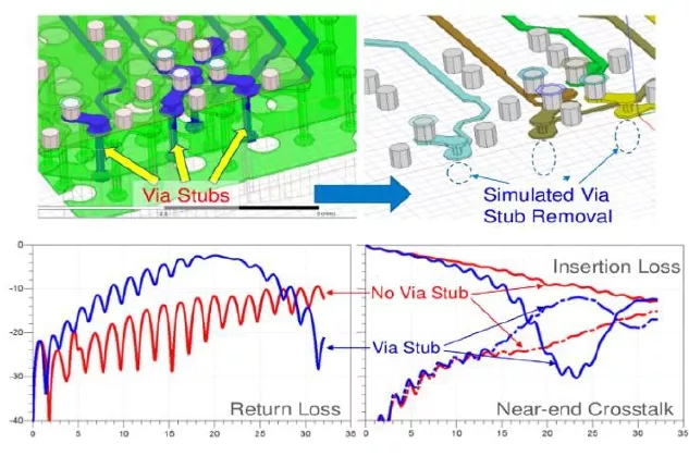
Figure 1: Via stubs significantly affect signal integrity
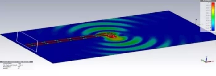
Figure 2: Without Via stitching, return current is broken
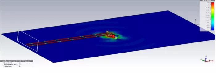
Figure 3: With Via stitching, return current is closed
To ensure robust signal recovery, designers must model the entire channel, including packages, vias, PCB traces, and connectors, with high accuracy. 3D electromagnetic (EM) simulation is essential to capture parasitic effects and discontinuities that impact highspeed signaling
Equalization Techniques for PCIe 5.0
To reopen the eye diagram and ensure a reliable sampling window at the receiver, PCIe 5.0 PHYs employ a combination of advanced equalization techniques:
- Feed-Forward Equalization (FFE): Pre-distorts the transmitted signal to counteract expected channel loss
- Continuous-Time Linear Equalization (CTLE): Amplifies high-frequency components at the receiver to compensate for low-pass channel behavior
- Decision Feedback Equalization (DFE): Uses previously received bits to cancel intersymbol interference (ISI) in real time
These techniques work in tandem to mitigate signal degradation and maintain compliance with PCIe 5.0 specifications.
Power Integrity (PI) in PCIe 5.0 Systems
Power Integrity (PI) is a critical design consideration in PCIe 5.0 systems due to the combination of high data rates (32 GT/s), low voltage swings (~800 mV), and tight noise margins. Inadequate PI can degrade signal integrity (SI), increase bit error rates (BER), and even cause link instability or failure. As data rates rise, the sensitivity of transceivers to power fluctuations increases significantly, making robust PI design essential
Key Challenges in PCIe 5.0 Power Integrity
- High Data Rates & Low Voltage Swing
The faster edge transitions required at 32 GT/s make the system more susceptible to power supply noise. Even minor fluctuations can introduce jitter and timing errors. - Tight Noise Margins & PSIJ (Power Supply-Induced Jitter)
With reduced voltage margins, any ripple or noise on the power supply can directly affect clock and data timing, leading to increased jitter and degraded eye diagrams. - Simultaneous Switching Noise (SSN) & Crosstalk
In high-lane-count configurations (e.g., x16), simultaneous switching of multiple drivers can induce noise on the power and ground planes, exacerbating insertion loss and inter-symbol interference (ISI).
Design Considerations for Robust PI
To ensure stable and reliable operation, designers must implement a well-architected Power Delivery Network (PDN) that minimizes noise and voltage fluctuations across the chip and its subsystems. Key strategies include:
- IR Drop Analysis
Evaluate voltage drops caused by resistance in power distribution paths to ensure sufficient voltage reaches all critical blocks. - Dynamic Voltage Drop Mitigation<
Account for transient voltage dips due to switching activity, especially during simultaneous lane transitions. - Ground Bounce Control
Minimize inductive effects in return paths that can cause ground potential shifts, particularly in densely packed I/O regions. - Decoupling Strategy
Optimize the placement and selection of decoupling capacitors to provide localized charge storage and suppress high-frequency noise. - Power Plane Design
Use wide, low-impedance power and ground planes with proper segmentation and stitching vias to reduce impedance and isolate noise sources.
Clock delivery and jitter in PCIe 5.0
Robust clock distribution is fundamental to achieving reliable SerDes performance in PCIe 5.0 systems, where data rates reach 32 GT/s. At these speeds, even minor timing variations can significantly impact signal integrity. The PCIe 5.0 specification imposes stringent requirements on transmitter (TX) jitter and eye diagram compliance, with an ideal eye width of just 31.25 ps, leaving little margin for error.
Sources of Jitter:
Jitter in PCIe systems originates from multiple sources, including:
- Reference Clock Noise
- Phase-Locked Loop (PLL)/Voltage-Controlled Oscillator (VCO) Phase Noise
- Clock Tree Skew and Crosstalk
- Package-Induced Jitter Amplification (e.g., from bumps and vias)
These sources contribute to both random jitter (Rj) and deterministic jitter (Dj), which must be carefully budgeted and controlled to meet the PCIe TX compliance mask.
Design Strategies for Jitter Mitigation
To ensure compliance with PCIe 5.0 jitter specifications, designers must adopt a systematic and hierarchical approach:
- Jitter Budget Allocation
Establish a detailed jitter budget early in the design phase, allocating allowable jitter to each subsystem (e.g., reference clock, PLL, clock distribution network). - Module-Level Performance Targets
Define and verify jitter performance at the block level to ensure each component meets its allocated budget. - System-Level Jitter Modeling
Perform end-to-end jitter simulations, including package and board-level effects, to validate compliance under worst-case conditions. - Low-Jitter Clock Topologies
Use differential signaling, short trace lengths, and impedance-controlled routing to minimize clock skew and noise coupling. - Power Supply Noise Isolation
Isolate clock generation and distribution circuits from noisy power domains using dedicated regulators, filtering, and decoupling strategies to reduce power supplyinduced jitter (PSIJ).
By prioritizing low-jitter design practices and integrating clock and power integrity considerations early in the development cycle, designers can ensure that PCIe 5.0 systems meet performance targets while maintaining power efficiency and system stability.
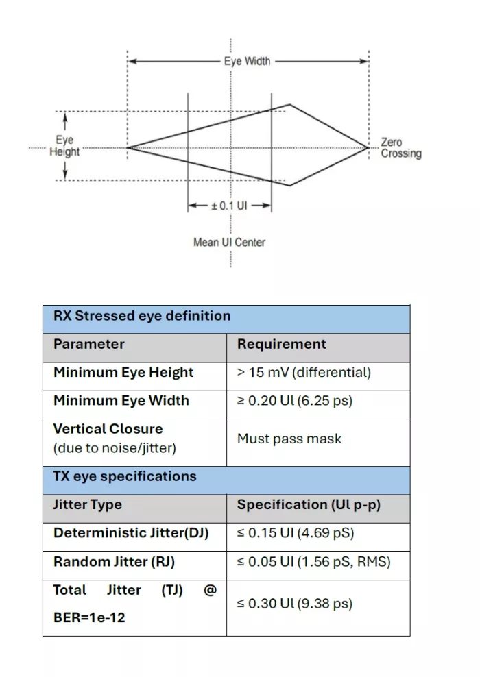
Figure 4: PCIe 5.0 RX Stressed Eye and TX Eye Specifications
By prioritizing low-jitter design practices and integrating clock and power integrity considerations early in the development cycle, designers can ensure that PCIe 5.0 systems meet performance targets while maintaining power efficiency and system stability.
Temperature cycling
In industrial environments, ambient temperatures can vary widely, typically from -40°C to +85°C. These fluctuations significantly impact the robustness of high-speed PCIe links, primarily due to changes in the resistivity, dielectric constant (Dk), and loss tangent (Df) of PCB substrates. These variations cause impedance drift, leading to reflections, signal distortion, and degraded eye diagram margins.
Elevated temperatures also exacerbate:
- Thermal noise
- Bandwidth reduction
- Increased inter-symbol interference (ISI)
- Amplified clock jitter
Material Performance Across Temperature
The following charts and table compare insertion loss across temperature for various PCB materials. The delta loss ranges from 18% to over 70%, depending on the material type and construction. These variations highlight the importance of selecting ultra-low-loss materials and leaving 10–20% design margin to account for environmental and manufacturing variability.
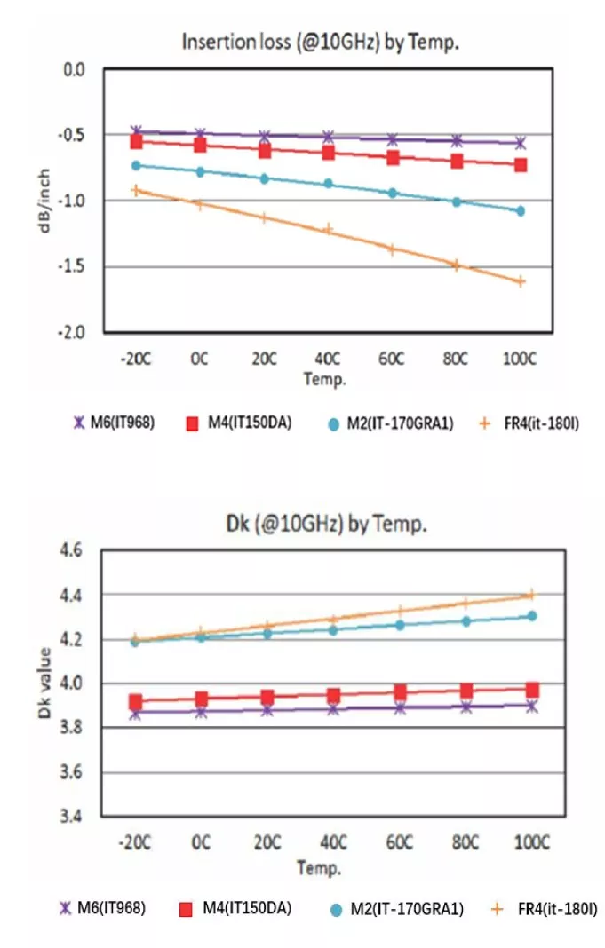
Figure 4: Channel Loss & DK vs Temperature Drift
| Material | -20°C | 0°C | 20°C | 40°C | 60°C | 80°C | 100°C | Loss Δ -20-100°C |
| M6(IT968) | -0.48 | -0.50 | -0.52 | -0.52 | -0.54 | -0.55 | -0.57 | 18.7% |
| M4(IT150DA) | -0.55 | -0.58 | -0.62 | -0.65 | -0.67 | -0.65 | -0.73 | 32.7% |
| M2(IT-170GRA1) | -0.73 | -0.78 | -0.84 | -0.87 | -0.95 | -0.87 | -1.08 | 48% |
| FR4(it-180I) | -0.93 | -1.03 | -1.13 | -1.21 | -1.38 | -1.49 | -1.61 | 73.1% |
Table 3: Summary of Insertion Loss
Mitigation Strategies
To maintain signal integrity across the full temperature range:
- Implement adaptive tracking algorithms and thermal drift compensation in the receiver
- Use temperature-stable materials with low Dk/Df variation
- Perform channel modeling under worst-case thermal conditions
- Validate performance with eye diagram analysis at temperature extremes
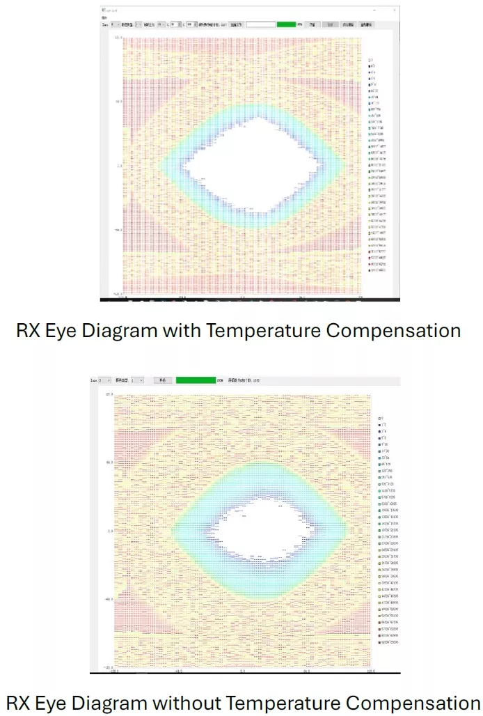
Figure 5: RX Eye Diagram with and without Temperature Compensation
Semiconductor process technology implications
As semiconductor manufacturing continues to advance, modern process technologies, such as FinFET and emerging GAA nodes, are scaling to ever-smaller geometries. While this scaling enables higher transistor density and improved performance, it also introduces a new set of challenges that directly impact PCIe 5.0 PHY design and overall system reliability.
Key Challenges of Advanced Process Nodes
- Increased Power Density & Self-Heating
Smaller geometries lead to higher power density, which exacerbates self-heating effects. This can degrade device reliability, reduce performance margins, and accelerate aging mechanisms such as electromigration and bias temperature instability (BTI). - Electromagnetic Interference (EMI) & Electrical Overstress (EOS)
Higher switching speeds and tighter integration increase susceptibility to EMI and EOS, especially in high-speed I/O like PCIe. These effects can cause transient faults, signal degradation, or permanent damage if not properly mitigated. - Process Variation & Mismatch
As feature sizes shrink, device mismatch becomes more pronounced, particularly in analog and mixed-signal circuits. This affects timing, gain, and offset characteristics, requiring on-chip calibration, adaptive tuning, and robust design-for- variation (DFV) methodologies.
Cross-Domain Optimization Strategies
To address these challenges, designers must adopt a holistic optimization approach that spans multiple domains:
- Die Architecture
Partition high-speed and sensitive analog blocks to minimize coupling and thermal hotspots. - Package Design
Use advanced packaging (e.g., flip-chip, 2.5D/3D IC) to reduce parasitics and improve thermal dissipation. - PCB Layout
Optimize trace impedance, via placement, and power/ground plane design to support high-speed signaling and power integrity. - Thermal Management
Integrate heat spreaders, thermal vias, and active cooling solutions to manage localized heating. - Connector and Interface Integration
Ensure mechanical and electrical robustness of high-speed connectors to minimize reflections and EMI.
These strategies require intensive simulation and modeling, including thermal-electrical cosimulation, EM analysis, and corner-case validation to ensure compliance with PCIe 5.0 performance targets under real-world conditions.
4. Silicon-Proven PCIe 5.0 Subsystem Solution
Innosilicon’s PCIe 5.0 IP offers a highly integrated, low-power, and low-latency solution designed for seamless SoC integration. Supporting PCIe Gen 1 through Gen 5, in both Endpoint (EP) and Root Complex (RC) modes, the IP is engineered for flexibility and performance across a wide range of applications. It supports multiple power modes for optimized power consumption, e.g., a PCIe link can be completely shut down if not used.
The IP adheres to the standard PCIe PIPE (PHY Interface for the PCI Express) specification, ensures interoperability and simplifies PHY-controller partitioning in complex SoC environments.
Key Features
- Broad Compatibility:
Supports backward compatibility with PCIe 1.0 through 5.0, enabling smooth integration into legacy and next-generation systems. - High Channel Loss Tolerance:
Capable of operating over channels with up to -36 dB insertion loss, supporting both Die-to-Die (D2D) and Long-Reach (LR) interconnects. - Integrated System Optimization:
Delivered as a hardened IP block with integrated I/O, ESD protection, and bump layout, reducing design complexity and silicon footprint. - Built-in DSP Cores:
Includes embedded digital signal processing (DSP) cores for adaptive equalization and calibration, eliminating the need for external CPUs or firmware. - On-Die Scope:
Used for measuring on-chip eye opening for system level debugging. - Modular Architecture:
Offers bypass mode and fine-grain equalizer tuning, allowing designers to optimize performance for specific use cases.
Application Suitability
This PCIe 5.0 IP is ideally suited for high-performance domains such as:
- Artificial Intelligence (AI)
- High-Performance Computing (HPC)
- Data Processing Units (DPUs)
- CXL Switches and Re-timers
Its support for dynamic bit-width, ultra-low latency, and power-efficient operation makes it a compelling choice for next-generation compute and connectivity platforms.
Platform-Aware Design with good margin for jitter tolerance
At PCIe 5.0 data rates (32 GT/s), jitter tolerance (JTOL) becomes a mission-critical metric for reliable system performance. The extremely tight signal integrity budgets at these speeds demand that PHYs not only meet but exceed the minimum JTOL specification across a broad range of sinusoidal jitter (SJ) frequencies.
A well-architected PCIe 5.0 PHY must incorporate platform-aware design techniques to ensure robust tolerance to timing deviations induced by system clocks, power supply noise, and interconnect variability. This includes careful optimization of the receiver’s clock data recovery (CDR) loop bandwidth, as well as inclusion of internal equalization and jitter tracking logic to maintain eye opening across varying link conditions.
One of the most sensitive systems use case is bifurcation, where the dynamic splitting of a single PCIe root complex into multiple logical links (e.g., 2×8, 4×4, or mixed (1×8 + 2×4) configurations). In such topologies, any deviation in link margin due to jitter can amplify crosstalk or skew issues, potentially degrading link training or causing intermittent failures.
To mitigate this, Innosilicon PCIe Gen5 PHY implementation demonstrates a healthy margin over the PCIe JTOL spec, as shown in the jitter tolerance plot. By tolerating higher SJ amplitudes than required across low to mid-frequency bands (where the receiver is most sensitive), the PHY design ensures platform-level resilience and interoperability, even in multi-slot or bifurcated environments.
The PCIe Gen5 PHY demonstrates an average jitter tolerance margin of over 120% across the full sinusoidal jitter frequency range, ensuring robust receiver performance well beyond the minimum compliance requirements
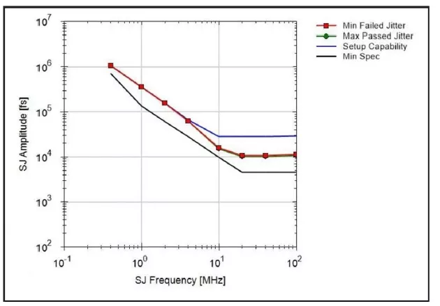
Figure 7: Innosilicon PCIe 5.0 JTOL Margin
Proven Silicon and Process Portability
The IP is silicon-proven across multiple foundries and process nodes, ranging from 28nm to 3nm, ensuring high reliability and broad deployment flexibility.
Comprehensive Bring-Up Support
To accelerate SoC validation and bring-up, Innosilicon assists with a test and debug platform, including:
- BERTs (Bit Error Rate Testers)
- High-speed oscilloscopes
- CBB = Chip Breakout Board, CLB = Card Level Board)Network and protocol analyzers
This comprehensive suite enables rapid debugging, compliance testing, and performance tuning during system integration.
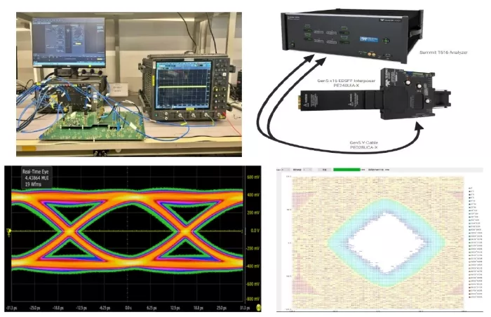
Figure 8: PCIe Compliance Test Equipment and Eye Diagram
5. Summary
The continued evolution of the PCI Express (PCIe) interface has made it a cornerstone of modern high-performance systems, offering scalable, efficient, and low-latency data transfer. With the advent of PCIe 5.0, the interface now supports a broad range of demanding applications, from HPC and AI to data centers, robotics, automotive, IoT, and networking.
As PCIe link speeds double with each generation, the associated design challenges grow in complexity. Key considerations such as signal integrity, power integrity, clock distribution, jitter, thermal variation, and process technology scaling must be addressed with a systemaware design approach. Each application presents unique constraints, requiring careful co-optimization across silicon, package, and board-level domains.
Innosilicon, with its proven track record in high-speed interconnect IP, offers silicon-proven PCIe 5.0 solutions that are optimized for performance, power, and integration. Their deep expertise and comprehensive support ecosystem have enabled customers to achieve PCIe compliance efficiently, even with limited resources. Looking ahead, Innosilicon remains committed to innovation in the PCIe domain, delivering best-in-class IP solutions that empower next-generation computing platforms with high bandwidth, low latency, and system-level reliability.
6. About Innosilicon
Innosilicon is a globally recognized leader in high-speed IP solutions and ASIC design services, offering both front-end and back-end capabilities. With a strong focus on accelerating time-to-market, reducing design risk, and optimizing cost, Innosilicon empowers customers with system-aware IP subsystems that seamlessly integrate into complex SoC designs.
Innosilicon’s Subsystem Offering
Founded in 2006, Innosilicon has built a reputation for reliability and innovation in the semiconductor industry. The company has supported over 300 top-tier clients, shipped more than 10 billion high-end SoCs, and delivered silicon-proven IP across advanced FinFET nodes at all major foundries, including TSMC, Samsung, and GlobalFoundries.
Industry Leadership & Innovation
Innosilicon is at the forefront of memory interface innovation, consistently pushing the boundaries of performance:
- First to achieve 24 Gbps GDDR6 using NRZ signaling
- LPDDR5X solutions delivering up to 10.7 Gbps, optimized for mobile and AI workloads
- System-aware subsystems combining high-speed I/O, world-class PHYs, and customizable controllers, ideal for large language models and data-intensive applications
Whether targeting AI, next-gen mobile, or edge compute, Innosilicon’s memory and interconnect IPs are designed to be fast, flexible, and future-proof.
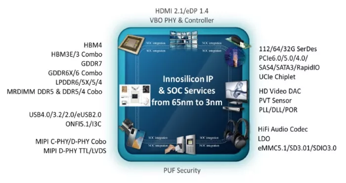
Comprehensive IP Portfolio
Innosilicon’s extensive IP offerings span a wide range of high-performance domains, including:
- Memory Interfaces: LPDDR6/5X/5, HBM4/3E, GDDR7/6X/6, MRDIMM DDR5, DDR5/4
- Interconnects: PCIe 6.0/5.0/4.0, UCIe Chiplet
- Applications: HPC, multimedia, automotive, AI, IoT, and more
With nearly two decades of experience, Innosilicon continues to drive innovation and deliver high-performance, low-power, and highly integrated IP solutions that meet the evolving demands of the semiconductor industry.
Innosilicon's IP Offering
Innosilicon Technology Inc.
97 E Brokaw Rd #210,
San Jose, CA 95112
For more information, contact sales@innosilicon.com
Related Semiconductor IP
- ASIL B Compliant PCIe 5.0 Integrity and Data Encryption Security Module (select configurations)
- PCIe 5.0 (Gen5) Standard Controller with AMBA bridge II
- PCIe 5.0 (Gen5) Standard Controller EP/RP/DM/SW 32-128 bits with AMBA bridge
- PCIe 5.0 (Gen5) Standard Controller EP/RP/DM/SW 32-128 bits
- PCIe 5.0 (Gen5) Premium Controller with AMBA bridge II
Related Articles
- Breaking the Memory Bandwidth Boundary. GDDR7 IP Design Challenges & Solutions
- TeraPool: A Physical Design Aware, 1024 RISC-V Cores Shared-L1-Memory Scaled-up Cluster Design with High Bandwidth Main Memory Link
- High Definition, Low Bandwidth -- Implementing a high-definition H.264 codec solution with a single Xilinx FPGA
- High-Speed PCIe and SSD Development and Challenges
Latest Articles
- RISC-V Functional Safety for Autonomous Automotive Systems: An Analytical Framework and Research Roadmap for ML-Assisted Certification
- Emulation-based System-on-Chip Security Verification: Challenges and Opportunities
- A 129FPS Full HD Real-Time Accelerator for 3D Gaussian Splatting
- SkipOPU: An FPGA-based Overlay Processor for Large Language Models with Dynamically Allocated Computation
- TensorPool: A 3D-Stacked 8.4TFLOPS/4.3W Many-Core Domain-Specific Processor for AI-Native Radio Access Networks