Virtual Prototyping Environment for Multi-core SoC Hardware and Software Development
NXP Semiconductors, Bangalore, INDIA
Abstract
The consumer electronic devices are becoming complex and employing multiple processors. Design of hardware and software for such a system presents lots of challenges. Hardware designer needs performance evaluation to select proper architecture. Software developer needs to develop and debug the software for multiple processors. In order to meet the competitive market, all this needs to be done even when the actual hardware is not available. This paper introduces a methodology based on Virtual Prototyping Environment, developed using simulation models of all the components of the target architecture. This methodology helps to fine-tune the hardware architecture as well as develop and debug the embedded-software.
1. Introduction
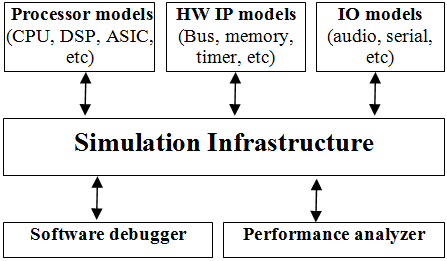
To meet high computational demands posed by latest consumer electronic devices (PDAs, cellphones, laptops, cameras, etc), current systems employ a multitude of processors[1] on a single chip. Figure 1 shows a typical multi-core SoC architecture with heterogeneous processors and the on-chip communication interconnect.
Along with the number of processors, their families also vary, like RISK, DSP, VLIW, multi-media, etc. As an example, high-end smartphones already contain a plethora of micro-processors (MPUs) and digital signal processors (DSPs) to provide advanced (2.75G and 3G) modem and application processing, as well as WiFi, GPS and Bluetooth functionality.

Fig 1. System-on-chip architecture
Developing, debugging and verifying multi-core embedded software (MCeSW) for such a system is a herculean task, taking up a big pie of the project budget. According to International Business Strategies (IBS), eSW development efforts now consume about 56% of the total SoC design effort. The challenges faced by design team are multiple and inter-related, like:
- maximum system-performance by partitioning the algorithm into software and hardware
- maximize productivity and reduce risk by re-use of legacy software
- meet time-to-market by developing new (and proprietary) software
- develop inter-processor communication (IPC) software for heterogeneous architectures
- meet power/performance constraints by proper planning of the resource usage
- ensure correctness through a good verification testbench
- chip is not fabricated yet
- complete board (chip with other peripherals) is not available yet
- board is not yet setup for usage in the lab
This paper presents a methodology involving high-level configurable simulation models of all the hardware IPs, enabling hardware-exploration, performance analysis along with software development and debug.
2. Related Work
The classic literature about multiprocessor systems provides all the basic concepts used in this work [2]
[3] explains top-down and bottom-up approaches for SoC design. Synthesis from system level models [4][5] and platform-based design [6] [7] are gaining wide acceptance for design of SoCs.
RAMP is the latest research accelerator for multi-core SoC platform [11]
Debugging a multi-core SoC is a tremendous challenge. In [12] MED (multicore embedded debugging) software tool is proposed that provides a virtual connection between the processor core in the SoC and its corresponding probe control.

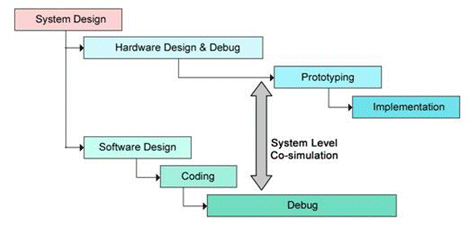
Fig 2. HW and SW development using VPE
3. Virtual Prototyping Environment
Virtual Prototyping Environment (VPE) is a high-performance, functional software model of an embedded system that is so complete that it fully mirrors the hardware functionality. Combining processors’ instruction-set simulators and high-level, fully functional C/C++ models of the hardware building blocks generates a VPE. The result is a high-level model of hardware,
sophisticated enough for an embedded-software developer to substitute for the physical device. Figure 2 shows how VPE enables parallel hardware and software developments. This technology enables concurrent software development at all levels, including ROM code, firmware code, device driver, OS porting, middleware and application development.
Typically, a VPE focuses on the functional aspects of the hardware (like functionality, memory maps, interconnects, etc), and typically avoids hardware details that are not exposed through the software programming model (like timing details, power dissipation, etc). However, these details can be included at the expense of simulation speed.
2.1. Essential components of a VPE
As discussed earlier, a VPE consists of high-level models of various components. These high-level models can be broadly categorized into the following:
-
Instruction Set Simulator (ISS): an ISS is capable of modeling CPU state and executing target program binaries. For achieving performance statistics, an ISS can be extended with a cache-model (to enable cache hit/miss numbers), pipeline-model (to enable stall, throughput statistics), etc.
-
Bus-protocol model: complete bus-protocol is reflected in the model, such as data-widths, transfer-timings, bus phases, device-selects, re-tries, bus turn-around after arbitration, etc. The bus-model can gather statistics like bandwidth, decode-errors, etc.
| Model | Configuration Parameters |
| Processor | L1 cache size, CPU clock speed, CPU/bus clock-ratio |
| Bus | Data bus size, number of Masters / Slaves, Pipeline depth, Multi layer, Address mapping, etc |
| DDR memory controller | Memory size, memory type, memory delay, arbitration scheme, etc Cache controller: L2 cache sizes, caching scheme |
| DMA controller | Service latency, throughput, etc |
| Interrupt controller | number of request lines, interrupt targets, priority levels, etc |
| Bus-bridge model | master bus protocol, slave bus protocol, number of slaves, clock domain crossing, etc |
Table 2. Performance statistics from models
| Model | Performance Statistics |
| Processor | instructions executed, trace, CPI, pipeline effects, etc |
| Bus | min/max/avg transfer latency, throughput ,transaction log, address-errors, etc |
| DDR memory controller | Efficiency, bandwidth per ID, Arbitration details |
| DMA controller | Transfer details, bandwidth, number of requests, etc |
| Interrupt controller | Interrupt rate, Request-to-service latency |
Functional peripheral models: the register interface, programming model, functionality and communication with other peripherals or its system I/O is modeled for each hardware peripheral. Modeling focus is on the interaction and impact between the software and the functionality of the peripheral. For example, programming of a certain control/command register of a DMA-controller governs the mode, direction, source and sink of DMA-traffic.
3. Applications of a VPE
A VPE is typically used for studying the architecture for different parameters, performing performance measurements, develop and debug of embedded software, etc.
3.1. Configurable System Architecture
VPE allows configuring the hardware architecture. Each functional model in the VPE can be made configurable through compile/run-time parameters. An eSW developer can actually develop the application focusing on a unique architecture or satisfying a family of architecture. Also, the eSW can be tested for its applicability in different system architecture. Obviously, a physical hardware board/chip does not such a facility. An indication of the configuration parameters[8] for models of typical IPs can be had from Table 1.
3.2 Performance Measurements
VPE allows measuring performance statistics[9] that are essential for improving the overall system. Typical statistics measured for a model are listed in Table 2.
3.3. Software Develop and Debug
VPE enables system-level software development as it uses the simulation models of the target processors. In order to have effective software development, it is necessary that the VPE simulates at a fast speed and allows software debug.
It is becoming more and more common for several cores[10] to be integrated to form a system-on-chip (SoC) in order to achieve optimum functionality and performance. The use of a RISC processor combined with a DSP is widespread, although other combinations are also employed. The debugging of SoC designs containing several cores places new demands on development tools and necessitates a multi-core debugger (MCD). An MCD allows debugging multiple core-models and hardware by synchronizing the operation of all cores during debug. Complex, multi-core systems can be stopped quickly to preserve critical state information, by providing a powerful cross core breakpoint facility that enables a breakpoint on one core to stop all other cores in the system.
4. Deployment of VPE
NXP-Semiconductors is actively using VPEs for software-development, performance-analysis and system-level simulations. Modeling-Group in Bangalore (India), within NXP-Semiconductors, has developed VPEs around various processors, like ARM7, ARM11, R.E.A.L. DSP, TriMedia, etc. As a use-case, NXP-VPE is discussed here.
NXP-VPE models the multi-core telecom subsystem for UMTS communication channels. The first design has been made largely depending on protocol decoding in hardware. Going forward, a more flexible design is required based on software implementations running on a vector processor. To prove the architecture in an early stage of the design-cycle, it is necessary to analyse the system design by developing and executing MCeSW over it.
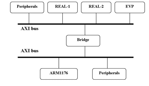
NXP-VPE is a multi-processor architecture that can be broadly divided into ARM subsystem and DSP-subsystem. Figure 3 shows the logical block-diagram of the modeled architecture. Due to confidentiality, all the IP-models that make up the VPE are not shown here. The bottom half makes the ARM-subsystem and the DSP-subsystem is at the top.
It should be re-emphasized that the NXP-VPE is functionally complete and simulates both on Linux and Windows. Figure 4 shows some of the tools used for VPE development under Linux and Windows.

Fig 3. NXP-VPE logical block-diagram
| Linux Packages | Version |
| /usr/bin/g++ | 3.2.3 |
| ADS | 1.2 |
| Expect | 5.38.0 |
| Gmake | 3.79.1 |
| OS version | Linux Enterprise version 3.0 |
| PERL | 5.6.0 |
| Windows Packages | Version |
| ADS | 1.2 |
| Micrososft Visual Studio | .NET 2003 |
| OS version | Windows XP |
Fig 4. Linux and Windows dev. environment
4.1. Simulation Speed
The simulation speed for NXP-VPE is measured by executing fixed-point FFT code on all the 4 cores simultaneously. Under this full system-load, the ARM subsystem is executing 70 Kilo-inst-per-second. This is a 1000-time faster than similar RTL-simulation.
4.2. Multi-core Debug
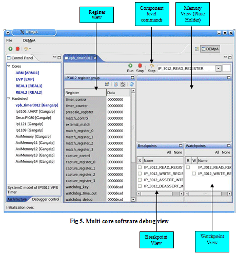
As NXP-VPE employs 4 cores in total, it is necessary that the MCeSW developer can simultaneously debug the applications running on all the cores and also view contents of peripheral IPs. Figure 5 shows the multicore-debug session in NXP-VPE. This debugger provides friendly user-interface with facilities like step/free -run simulation mode, register view, memory view, breakpoints view, watch-points view.

5. Conclusions
This paper highlighted a methodology for exploring multi-core system-level architecture and developing software even in the absence of target hardware. This methodology is termed Virtual Prototyping Environment and is being actively pursued at the Modeling-Group in Bangalore (India) within NXP-Semiconductors. As a concrete use-case, this paper presented a complex VPE developed for the multi-core telecom subsystem. The VPE is being successfully used within NXP for the multi-core embedded software development and architecture exploration. All of this happens while the architectural spec and hardware design are still being finalized!
6. References
[1] A. Jerraya, W. Wolf, “Multiprocessor Systems-on-Chips”, Morgan Kaufmann Series in Systems on Silicon
[2] D.E. Culler, J. Pal Singh, ”Parallel Computer Architecture,” Morgan Kaufmann Publishers, 1999
[3] K. Keutzer, “A Discipline.d Approach to the Development of Platform Architectures,” Synthesis and System Integration of Mixed Technologies, Nara, Japan, October 2001
[4] R. Ernst, et al., “The COSYMA environment for hardware/software cosynthesis of small embedded systems,” Microprocessors and Microsystems, 1996
[5] F. Balarin, et al., “Hardware-Software CO-desilp of Embedded Systems: The POLIS approach,” Kluwer Acadmnic Press, 1997
[6] Cadence Design Systems, Inc., Virtual Component Co-design: http://www.cadence.coduroducts/vcc.html
[7] K. Keutzer, et al., “System-level design: orthog;onalization of concerns and platform-ba:jed design,” IEEE TCIAD, Dec. 2000
[8] J. Hennessy and D. Patterson, “Computer Architecture: A Quantitative Approach”, Morgan Kauffman
[9] R. Jain, “The Art of Computer System Performance Analysis”, John Wiley & Sons
[10] P. Enslow. Multiprocessor Organization Survey. ACM Computing Survey, 9(1), 1977
[11] Patterson, D.A., “RAMP: research accelerator for multiple processors - a community vision for a shared experimental parallel HW/SW platform.” IEEE Int’l Symp. Performance Analysis of Systems and Software, 2006
[12] Leatherman, R. Stollon, N., “An embedding debugging architecture for SOCs” IEEE Potentials, Feb 2005 Volume: 24 , Issue: 1
Related Semiconductor IP
- Ultra-Low-Power LPDDR3/LPDDR2/DDR3L Combo Subsystem
- Parameterizable compact BCH codec
- 1G BASE-T Ethernet Verification IP
- Network-on-Chip (NoC)
- Microsecond Channel (MSC/MSC-Plus) Controller
Related Articles
- How to make virtual prototyping better than designing with hardware: Part 1
- Dealing with automotive software complexity with virtual prototyping - Part 1: Virtual HIL development basics
- Dealing with automotive software complexity with virtual prototyping - Part 3: Embedded software testing
- Interstellar: Fully Partitioned and Efficient Security Monitoring Hardware Near a Processor Core for Protecting Systems against Attacks on Privileged Software
Latest Articles
- Lyra: A Hardware-Accelerated RISC-V Verification Framework with Generative Model-Based Processor Fuzzing
- Leveraging FPGAs for Homomorphic Matrix-Vector Multiplication in Oblivious Message Retrieval
- Extending and Accelerating Inner Product Masking with Fault Detection via Instruction Set Extension
- ioPUF+: A PUF Based on I/O Pull-Up/Down Resistors for Secret Key Generation in IoT Nodes
- In-Situ Encryption of Single-Transistor Nonvolatile Memories without Density Loss