Design and Implementation of an OCP-IP Compliant 64-Node Butterfly Network on Chip on Multi-FPGA
Khawla Hamwi, Omar Hammami (ENSTA ParisTech)
Abstract :
There is a growing demand of high-performance computing systems to cope with increasing data size and amount of arithmetic operation in various scientific computations. On top of this, several multi-FPGA systems have been proposed as reasonable methods to efficiently solve large scale application which adopt extremely iterative algorithms or use large-scale data that cannot be loaded onto one FPGA. In this paper, we report the design and multi- FPGA chip implementation of a 64-node butterfly network based on MPSOC. Our Network is placed and routed automatically on the 4 FPGA included in Eve Zebu-UF4 platform.
I. INTRODUCTION
International Technology Roadmap of Semiconductors (ITRS) projects that hundred of processors will be needed for future generation MPSOC designs [1]. Additionally, FPGAs are commonly used as platforms for hardware acceleration via application-specific architectures. However, for large, complex applications a single FPGA does not provide sufficient resources for a complete implementation in hardware. This led to the development of scalable multi-FPGA platforms that provide sufficient resources for implementing these types of systems.
The remainder of this paper is organized as follow: in the next section we define the butterfly network and present our 64-node butterfly network. Section III explains the design methodology. The implementation results will be presented in the section IV where section V concludes our paper.
II. BUTTERFLY ARCHITECTURE
Butterfly network is the quintessential indirect network. The butterfly topology has the minimum diameter for an N node network with switches of degree S=2k, H=logk N+1. However, the logarithmic diameters and simple routing of the butterfly network made it and its variants some of the most popular of interconnection network for many applications [2].
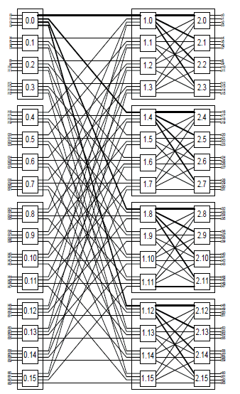
Figure 1. A 64-node butterfly network
Figure 1 shows a 64-node butterfly network in which data flows from the input nodes on the left through three stages of switch nodes (rectangle) to the output nodes on the right. The switch nodes are labeled with their stage and address. All channels are unidirectional from the left to the right.
III. DESIGN METHODOLOGY
MPSoC has become a much more prevalent design style, to achieve tight time-to-market design goals, to maximize design reuse, to simply the verification process and to provide flexibility and programmability for post-fabrication reuse of complex platforms. Figure 2 shows the design flow which will be explained in the following subsection, and then we will briefly present the tools which are used to achieve it.
A. Design flow
At the beginning, architecture is designed manually by using Arteris NoC Solution [3]. In this tool, interface units protocols are configured then the architecture is realized using switches and route tables.
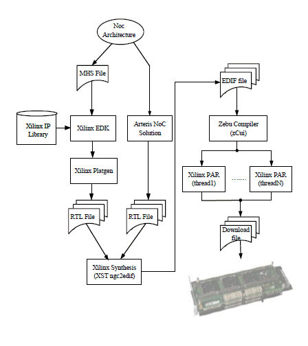
Figure 2. MPSOC design flow
Once the design is finished, it is tested to verify the connectivity and configuration after that a VHDL NoC file is generated. With the NoC VHDL code imported as an IP to the EDK environment, the MPSoC design can take place, where MicroBlaze processors and other memories are added using Xilinx IP library as illustrated in Figure 2. The NoC connection (with its OCP interface unknown to EDK) is realized through direct access to MHS hardware description file. At the end of this phase two types of files are generated (1) Netlist (.ngc) files for hardware description (2) executable and linked (.elf) files for MicroBlaze processors. The NGC files from the previous phase are converted into Electronic Design Interchange Format (EDIF) then used in Eve Zebu Compiler for partitioning of the design on the 4 available FPGAs if necessary.
B. Arteris NoC Solution
Arteris NoC Solution addresses the needs of complex designs which require very high performance and a broad range of advanced interconnect features. With Arteris NoC Solution, the SoC designers can quickly configure, instantiate, and connect with drag-and-drop ease various Intellectual Property (IP) elements to construct a NoC optimally suited for the application. In addition, they can use different protocols for on-chip communication interface such as Open Core Protocol (OCP-IP), Advanced High performance Bus (AHB) and Advanced eXtensible Interface (AXI) [3].
The essential building block of the NoC interconnect system is the switch generator which has the following main features: (1) fully synchronous operation, (2) internal full crossbar: up to one data word transfer per MINI port and per cycle, (3) full throughput arbitration: up to one routing decision per input port and per cycle, wormhole routing to reduce latency, (4) freely cascading connection, supporting any loop-less network topology. It is possible to select the arbitration type of the switch among 4 possible values Round-Robin, LRU, Random, FIFO with default value Round-Robin. Several optional registers can be added in order to pipeline the switch. Because of the constraints between different options, there are 80 different configurations for each switch [9].
C. Embedded Development Kit (EDK)
The Xilinx EDK [4] is a suite of tools and IP that enables to design a complete embedded processor system for implementation in a Xilinx FPGA device. The Microblaze processors which represent the principal EDK components, have internal memory of 32 KB for data (data local memory bus, dlmb) as well as instruction (instruction local memory bus, ilmb). The MicroBlaze hardware system is defined in a textbased Microprocessor Hardware Specification (MHS) file where we can set all of our system hardware parameters [6].
D. Eve Zebu Compiler (zCui)
Eve Zebu Compilation Graphical Interface (zCui) is a compilation tool produced by EVE Company. In our work, we use this tool for Eve Zebu-UF4 (Ultra Fast) compilation whereas its main steps are listed below [5]:
- Preparation the design for emulation:
- Memory modeling.
- Clock modeling.
- Verification environment description using a proprietary “Design Verification Environment” file (DVE).
- Synthesis RTL design by using Zebu RTL front-end which is integrated in (zCui).
- Compilation:
- Mapping of the design.
- System level place and route.
- Xilinx ISE place and route.
- Configuration of the Reconfigurable Test Bench (RTB) according to the test environment.
- Xilinx ISE place and route for each RTB FPGA netlist.
- Manual optimization of clustering.
- Addition of debug features according to architecture and performance requirement.
E. Eve Zebu-UF4 Platform
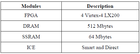
Eve Zebu-UF4 platform is based on 4 Xilinx Virtex-4 LX200, built as an extended PCI card via a motherboard daughter card approach.
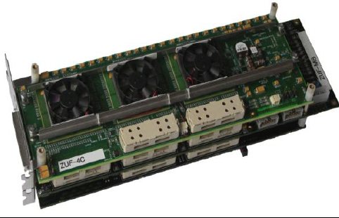
Figure 3. Eve Zebu-UF4 platform
The 4 FPGA based system can emulate the equivalent of up to 6 million ASIC gates in a single card. Eve Zebu-UF4 also includes on-board memory capacity based on 64 Mbytes of SSRAM and 512 Mbytes of DRAM memory chips via an additional memory board, which plugs into the PCI motherboard.
TABLE I. EVE ZEBU-UF4 PLATFORM DETAILS
IV. DESIGN IMPLEMENTATION
In our design implementation, Microblaze softcore processors are used as masters and Block RAM (Random Access Memory) are used as slaves. Each MicroBlaze processor [6] is configured to its Full configuration and is given additional local 32KB BRAM memory connected (Figure 4 ) via 2 LMB BRAM Memory Controllers using 2 LMBs (Local Memory Bus) to provide Instruction Memory (via ILMB port) and Data Memory (via DLMB port). The MicroBlaze is connected via two FSLs (Fast Simplex Bus) into a FSL2OCP unit which converts the FSL into OCP interface that is connected to one of the NoC Master OCP NI interfaces.
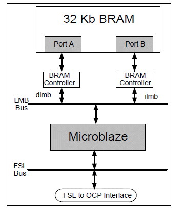
Figure 4. Microblaze connection
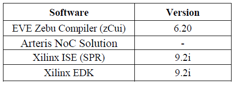
MicroBlaze processors are connected to switches through Network Interface Units (NIUs). To increase the compatibility and to ease the reutilization of the architecture, the OCP-IP standard is used for the connection of MicroBlaze and NOC. Several EDA tools are used in our design. These tools with its version are shown in Table II.
TABLE II. DESIGN TOOLS VERSIONS
Additionally, several IPs are used in the design of MPSoC and its names with its versions are shown in Table III. All the IPs are from Xilinx which are available in the EDK except 2 IPs developed by our team work in ENSTA [8]. These IPs are developed for the OCP-IP interface to the MPSoC system in the EDK.
TABLE III. UESED IPS VERSIONS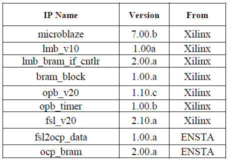
The 64-node butterfly network is implemented on Eve Zebu-UF4 platform which bases on 4 Xilinx Virtex-4 LX200. The place and route between these 4 FPGA is achieved automatically and the results are presented in Table IV.
TABLE IV. LOGIC UTILIZATION OF POST-PLACE AND ROUTE OF THE BUTTERFLY NETWORK ON 4 FPGA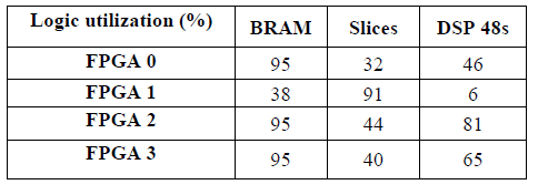
The resulting floorplan is shown in Figure5.
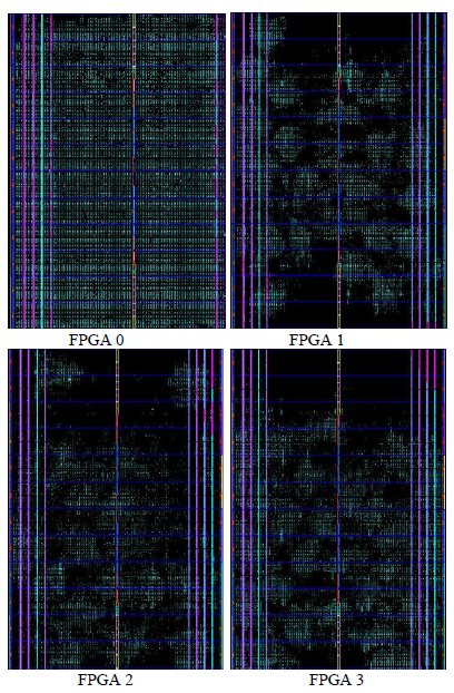
Figure 5. Floorplan of 64 PE SoC on Eve Zebu-UF4 platform
This 64 Processing Element (PE) butterfly architecture will be used for parallel Fast Fourier Transform (FFT) software implementation in order to avoid hard IP implementation [13-15].
V. CONCLUSION
We reported in this paper the complete design and implementation of a multi-FPGA chip butterfly NOC based MPSOC. OCP-IP interfaces have been used between PE and NOC NIU and between NOC NIU and local memories. This design methodology allows our design to be PE independent. In the future work, we will use our design to study an application like signal processing algorithms. Also, we can implement our butterfly NOC on other Multi-FPGA platforms and compare the results.
REFERENCE
[1] ITRS http://www.itrs.net/
[2] W.J.Dally,and B.Towles, “Principles and Practices of Interconnection Network”, Morgan Kaufmann puplishers,2004.
[3] Arteris http://www.arteris.com/
[4] EDK Concept, tool, and Technique, available on www.xilinx.com/support/documentation/sw_manuals/edk10_ctt.pdf
[5] ZeBu-UF Compilation Manual, Version 4.2_x, Dec 2009, Eve.
[6] MicroBlaze Processor Reference Guide, available on www.xilinx.com/support/documentation/sw_manuals/mb_ref_guide.pdf
[7] OCP-IP OCP-IPOpenCoreProtocolSpecification2.2 . http://www.ocpip.org/home , 2008.
[8] Z.Wang, and O.Hammami, “External DDR2-constrained NOC-based 24-processors MPSOC design and implementation on single FPGA”, Design and Test Workshop, 2008. IDT 2008. page(s): 193 – 197, 2008.
[9] X.Li and O.Hammami, “Multi-FPGA Emulation of a 48-Cores Multiprocessor with NOC”, Design and Test Workshop, IDT 2008, pp.205-208, 2008.
[10] XilinxVirtex-4 http://www.xilinx.com/support/documentation/virtex-4.htm
[11] Xilinx EDK9.2
[12] Xilinx ISE9.2
[13] Fast Fourier Transform (FFT) IP Core for FPGA and ASIC. Available on: http://www.dilloneng.com/fft_ip
[14] Datesheet for FFT Core. Available on: http://www.softjin.com/IP_Datasheet_PDF_version/FFT_datasheet.pdf
[15] LogiCORE IP Fast Fourier Transform V7.1. available on: http://www.xilinx.com/support/documentation/ip_documentation/xfft_ds260.pdf
[16] FFT0064- 64 point FFT core. Available on: http://www.ipcores.com/64PointFFT.html
Keywords- Multi-FPGA; NoC; Butterfly network; MPSOC; Eve Zebu-UF4 Platform.
Related Semiconductor IP
- Ultra-Low-Power LPDDR3/LPDDR2/DDR3L Combo Subsystem
- 1G BASE-T Ethernet Verification IP
- Network-on-Chip (NoC)
- Microsecond Channel (MSC/MSC-Plus) Controller
- 12-bit, 400 MSPS SAR ADC - TSMC 12nm FFC
Related Articles
- A 24 Processors System on Chip FPGA Design with Network on Chip
- Modelling OCP Interfaces in SystemC: Standards built on top of OSCI's TLM-2
- Survey of Chip Designers on the Value of Formal Verification Across the Spectrum of Applications
- Using non-volatile memory IP in system on chip designs
Latest Articles
- Extending and Accelerating Inner Product Masking with Fault Detection via Instruction Set Extension
- ioPUF+: A PUF Based on I/O Pull-Up/Down Resistors for Secret Key Generation in IoT Nodes
- In-Situ Encryption of Single-Transistor Nonvolatile Memories without Density Loss
- David vs. Goliath: Can Small Models Win Big with Agentic AI in Hardware Design?
- RoMe: Row Granularity Access Memory System for Large Language Models