Interface Synthesis in Multiprocessing Systems-On-Chips
and Marcello Lajolo from NEC Laboratories America - Princeton, NJ
Abstract
Although Moore’s Law, in principle, enables a huge number of components to be integrated into a single chip, design methods that will allow system architects to put the components together to achieve cost, power and time-to-market targets are severely lacking. System-level design and optimization techniques can significantly reduce the design gap by providing solutions that achieve correct-by-construction approach rather than the correct-by-iteration approach. This paper presents a programmatic interface generation tool for automating the generation of the hardware/software interfaces in the context of multi-processor Systems-On-Chips. The solutions that we present are of crucial importance in a platform based design environment for building a flexible system with reusable IPs and CPU cores.
1 Introduction
The growing number of SOC (System-On-Chip) developments has highlighted for many systems companies the problems associated with parallel development of hardware and software. Well understood hardware and software development programs may exist happily in isolation, but bringing them together in a successful SOC development that is firsttime functional and enters the market when planned is proving to be a challenge. A solution to these difficulties exists and it could allow design teams to report huge savings in system integration time by concurrent development of hardware, software, documentation and testing. By capturing project data in a structured database, all developments can continue in isolation with confidence that the entire design team is working with appropriate yet consistent design files. The approach also ensures the ability to make late changes or fix original specification errors consistently across the development team.
The rest of the paper is organized as follows. Section 2 describes our philosophy for IP core integration. Section 3 describes the basic components of our customizable multiprocessor architecture, such as basic single processor platform, bridge and arbiter. Section 4 gives an overview of our multiprocessor mapping strategy. In section 5 we present some examples of multi-processor mapping. Section 6 concludes the paper.
2 IP Core Integration Philosophy
In a typical SOC architecture, an embedded processor executes software that controls the system setup and operation (see Fig. 1). The processor’s view of the system takes the form of a series of interface points in its address space. These interface points correspond to registers within each of the IP blocks and usually take the form of memory-mapped registers connected to the processor via the system bus. A complex SOC often comprises multiple processors, DSP cores, or both. These cores may share a common bus, or the chip may contain a more intricate bus bridge for sharing data.
Figure 1 shows our proposed philosophy for IP core integration. The core is considered as partitioned in three sub-parts: the transaction-level model (TL) describing its functionality, an event support mechanism that provides a portable protocol for IP core integration and finally a bus interface which acts as an adaptation layer to connect the core to a specific bus architecture. Ideally, if the bus architecture changes, only the bus interface should change, while the other two layers should remain unaffected.
By using a common description of the registers between hardware and software, development teams can ensure that, as the design of an IP block matures, the detailed hardware model can replace the simple register model and that they can easily rerun software tests. A common description also ensures no surprises upon hardware and software integration in latter development stages. Even more important, automating the creation of these low-level functions on both the hardware and the software sides allows valuable engineering resources to concentrate on adding value to the product.
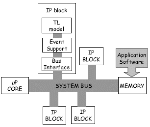
Figure 1: Core-based SOC architecture.
3 Multi-processor architectural template components
Our approach for automatic mapping on multi-processor architectural templates considers a multi-processing environment as a composition of multiple single-processing units as the one shown in Figure 2.
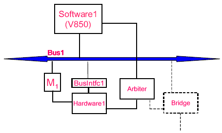
Figure 2: Single-processor platform.
It is a bus-based system consisting of one NEC V850 CPU and one hardware unit (user-defined logic) connected to the bus using a dedicated bus interface. A memory module (M1) is attached to the bus and is used for storing the application software as well as for implementing memory-mapped hardware/software communication. Bridges can be used in order to connect different processing units of this kind. CPU, hardware unit and bridges can all act as masters on the bus and hence an arbitration unit is required. In [1] we presented an automatic synthesis of hardware/software interfaces for this kind of architecture that is a core component of the work herewith described.
3.1 Bridge
A bridge is a device used to connect a primary bus with a secondary bus. The architecture of our bridge is shown in Figure 3. It is a bidirectional bridge composed of two identical unidirectional bridges used for implementing both upstream and downstream connections. Upstream connections are the ones originated on the primary bus (Bus Up) and directed toward the secondary bus (Bus Down). Downstream connections are the ones going in the opposite direction.
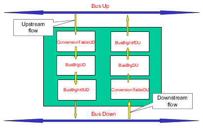
Figure 3: The architecture of our bridge.
ConversionTableUD is an internal memory unit containing the set of addresses that the bridge has to capture on the primary bus and propagate to the secondary bus. On the other side, ConversionTableDU contains the set of addresses that have to be captured on the secondary bus and propagated to the primary bus. These tables are automatically configured by our interface synthesis tool as it will be shown later.
BusBrgUD and BusBrgDU describe the behavior of the bridge for both read and write transactions. We have used for both blocks the finite state machines shown in Figure 4, but different behaviors could be implemented.
Finally, BusBrgIntfUD and BusBrgIntfDU are the adaptation layers used to connect the bridge to the secondary and primary bus, respectively.
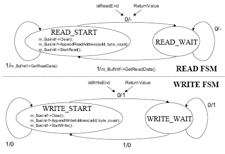
Figure 4: Finite state machines for the bridge.
3.2 Arbiter
The bus used in our basic single-processor platform requires an arbitration process since multiple components connected to it can act as masters and hence initiate a transaction. In particular, possible masters are the CPU, the bridge, and all the hardware tasks. Before a bus master can execute a transaction, it must request and be granted the use of the bus. Each bus master has a pair of REQ# and GNT# signals connecting it directly to the central arbiter. When a master wishes to use the bus, it asserts the REQ# signal. Sometime later the arbiter will assert the corresponding GNT# signal indicating that this master is next in line to use the bus. Several bus arbitration policies can be used (e.g. round robin (no priority), static priority, ...).
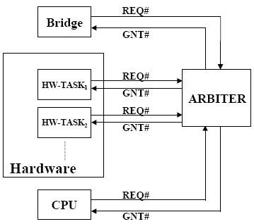
Figure 5: Bus arbiter.
4 Multi-processor mapping strategy
Figure 6 shows an example of multi-processor architectural template that utilizes the single-processor platform of Figure 2 as a basic component. Bridges are used in order to route a connection from one bus to another. The architecture is a hierarchical bus-based system with two NEC V850 CPUs and three hardware units. Bu83, in this example, does not have any processor connected to it. Different address ranges, configurable by the user, are associated to every bus for memory-mapped communication.
In our mapping strategy, a multi-processor architecture is seen as a collection of multiple single-processor units. Mapping is initially performed separately on each processing unit using the technique presented in [1]. Connections across different processing units are then routed through the bridges and address conversion tables (hashes) are generated for all the bridges.
The basic idea is that once the functionality of the system to be implemented has been partitioned (distributed) among the different hardware and software processing units available on this architectural template, a certain number of connections between different tasks will be created. A generic connection is characterized as shown in Figure 7. Connections between tasks mapped on the same single-processor unit will not require any bridge, while connections between tasks mapped on different single-processor units will utilize a certain number of bridges. For each connection, we store in an internal database the sequence of bridges involved in its implementation.
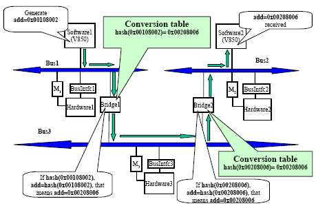
Figure 6: Dual-processor platform.

Figure 7: Connection characterization.
The way in which automatic mapping gets implemented in our methodology is by configuring each bridge with a specific address conversion table. The basic strategy is the following:
- Single processor mapping has initially generated an address (source) for the signal on the source bus.
- 2. If the signal is directed toward a different processing unit (bus), an address (dest) has also been generated for the same signal on the destination bus.
- 3. The conversion table of the first bridge encountered on the communication path is updated in order to convert the source address in its corresponding destination address: Hash(source)=dest
- All other bridges encountered afterwards will simply propagate that communication without changing its address: Hash(dest)=dest
Figure 8 shows the pseudocode of our mapping algorithm for a generic multi-processor architecture. The inputs to the algorithm are: a file containing the entire functional netlist of the system with the set of modules and their interconnections (netslist.star), a data structure (connection[Nc], where Nc is the number of connections) containing the source and destination modules for a specific connection, as well as the source and destination addresses and the list of bridges involved, and an array containing a string representing the implementation of all the functional modules (implem[Nm], where Nm is the number of modules).
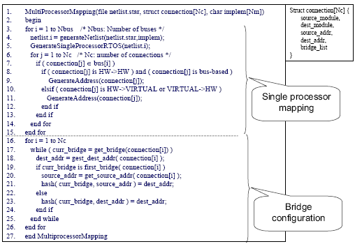 Figure 8: Pseudocode of the mapping algorithm.
The algorithm consists of two main loops. The first loop (lines 3-15) is performed on the number of buses Nbus and, for each of them, a customized netlist file, netlist.i, is generated (line 4). This is a generic description for a singleprocessing unit that supports only three possible implementations: HW, SW or VIRTUAL. For example, when considering the CPU called Software1, all modules implemented on it will have an implementation of type SW, while modules implemented on Hardware1 will have an implementation of type HW. All other functional modules implemented on different architectural units (Software2, Hardware2, Hardware3) will have an implementation of type VIRTUAL. The file netlist.i is then passed as an argument to the function GenerateSingleProcessorRTOS (line 5) that will generate an operating system for the i-th CPU based on specific addresses (or interrupt lines) assigned to all HW-SW and SWHW connections. For this RTOS, all VIRTUAL components are considered as implemented in HW, and hence for SWVIRTUAL and VIRTUAL-SW communication addresses are generated, while HW-VIRTUAL and VIRTUAL-HW communications are considered as point-to-point communications and no addresses are generated in this stage.
Then, the nested loop at lines 6-14 scans all the connections involved with the current bus. Those connections are extracted from the global list of connections at line 7. The purpose of this nested loop is to check whether additional addresses need to be generated. This is the case for HW-HW connections implemented as bus-based communications (lines 8-9) andHW-VIRTUAL and VIRTUAL-HW communications (lines 10-11). The if conditions tested at lines 8 and 10 make use of the implem input data structure in order to check the implementation of the source as well as the destination of the current connection. The new addresses are selected among the ones still unused in the range of addresses associated to the current bus. This is done by the function GenerateAddress. (lines 9 and 11) that receives as input parameter the name of the connection. At the end of this phase all connections have been characterized with a source and a destination address.
The second and last loop (lines 16-26) then scans again all connections in the system in order to prepare the address conversion tables for all the bridges. For each connection, the entire list of bridges involved in the connection is scanned. For the first bridge in the list, the one closer to the source module, the hash table will convert the source address in its destination address. All the subsequent bridges will simply propagate the destination address.
5 Multi-processor mapping, a case study
In this section we show a couple of mapping examples for the system shown in Figure 9 that represents a simple matrix multiplication algorithm consisting of three processes: the Index Control, that controls the execution of the algorithm, the Data Retriever, which fetches data from the shared memory and accumulates intermediate results, and the Multiplier, that multiplies two numbers at a time.
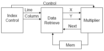
Figure 9: Matrix multiplication system.
5.1 First mapping example
Figure 10 shows a first example of mapping in which Index Control and Multiplier are implemented as software running on CPU1, while Data Retrieve is implemented as software running on CPU2. The configuration of the memory-mapped regions that has been specified is shown in Figure 11. The address space reserved for Bu81 starts at 0x100000, the one reserved for Bu82 starts at the address 0x200000 and the one forBu83 at 0x300000.
In this example, the total number of buses is three, so there will be three iterations of the single processor mapping loop (lines 3-15) of the algorithm of Figure 8. The first iteration of the loop generates the netlist file (netlist.1) for Bu81 in which for Index Control and Multiplier the implementation will be
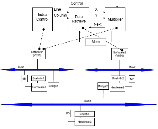
Figure 10: First mapping example.
SW, while for Data Retrieve, the implementation will be VIRTUAL, as this task is not mapped on Bu81. Since in this case there are neither HW-HW connections, nor HW-VIRTUAL or VIRTUAL-HW connections, all the required addresses have already been generated after the execution of the function GenerateSingleProcessorRTOS and the inner loop at lines 6-14 does not generate any additional address. The result of this iteration is the set of addresses starting with 0x1 in Table 1.

Figure 11: Configuration of memory-mapped regions.
The second iteration of the single processor mapping loop generates the netlist file (netlist.2) for Bu82 in which for Index Control and Multiplier the implementation will be VIRTUAL while for Data Retrieve, the implementation will be SW. As in the first iteration, the function GenerateSingleProcessorRTOS generates all the required addresses and the inner loop at lines 6-14 does not generate any additional address. The addresses generated for this bus are the ones starting with 0x2 in Table 1.
Since there are no tasks on Bu83, the third iteration of the single processor mapping loop is not relevant. The final situation is presented in Table 1 where for each signal connecting tasks mapped on different single-processor platforms, there are two addresses associated: the source and the destination address.
The bridge configuration loop at lines 16-26 in the algorithm in Figure 8 is now executed in order to scan all connections and prepare the address convertion tables for all the bridges. The signals Line, Column and Next, are generated on CPU1 and then go to CPU2, passing through Bu81(the first bus), Bridge1, Bu83, Bridge2 and Bu82 (the last bus). For all these signals, the first bridge encountered is Bridge1. In this bridge the source address is converted in its destination address, while in the second and last bridge encountered, Bridge2, the address remains unchanged.
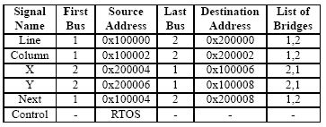
Table 1: Address table for the first mapping example.
The situation for signals X and Y is similar, but source and destination modules are inverted with respect to the previous signals and hence the sequence of buses and bridges encountered in their transfer is also inverted. As a consequence, the memory-mapped address masks in their source and destination addresses are swapped. Finally, for the $&%('*F0-<%<6 signal, both source and destination modules are implemented as software running on the same CPU and hence the communication is handled by the RTOS using a shared variable, and no memory-mapped address is generated.
5.2 Second mapping example
Figure 12 shows another example of mapping in which Index Control is implemented as software running on CPU1, Data Retrieve as hardware connected to Bu82 and Multiplier as hardware connected to Bu81.
As in the previous example, the first iteration of the singleprocessor mapping loop generates the netlist file (netlist.1) for Bu81 in which for Index Control the implementation will be SW, the Multiplier will be HW, while for Data Retrieve the implementation will be VIRTUAL, as this task is not mapped on Bu81. In this case, Next is a HW-VIRTUAL connection, while X and Y are VIRTUAL-HW connections. The addresses for these three connections are not generated by the function GenerateSingleProcessorRTOS. They are generated, instead, by the inner loop at lines 6-14, that assigns one address, selected among the ones still available, to all the connections left unmapped by the function GenerateSingleProcessorRTOS . The result of this iteration is the set of addresses starting with 0x1 in Table 2.
The second iteration of single-processor mapping loop generates the netlist file (netlist.2) for Bu82, in which for Index Control and Multiplier the implementation will be VIRTUAL, while for Data Retrieve the implementation will be HW. Since
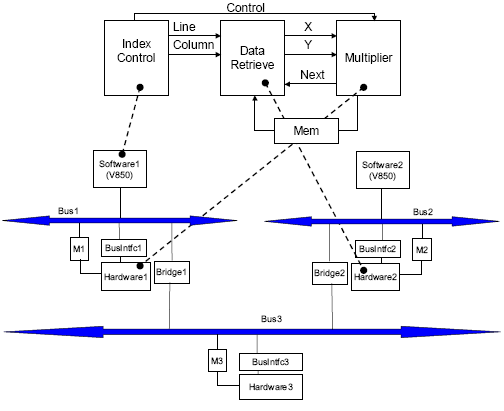
Figure 12: Second mapping example.
in this case there are only VIRTUAL-HW and HW-VIRTUAL connections, the function GenerateSingleProcessorRTOS does not generates any address: all of them are assigned by the inner loop at lines 6-14 that generates the source address for signals and and the destination address for signals Line, Column and Next. The Control signal, in this iteration, does not get involved, since it is a communication that is mapped exclusively on Bu81 and hence here it is classified as a VIRTUAL-VIRTUAL connection. The addresses generated for this bus are the ones starting with 0x2 in Table 2.
As in the previous mapping, the third iteration of the single processor mapping loop is not relevant, since there are no tasks on Bu83. At this point, the bridge configuration loop will configure the address conversion tables for all bridges based on the mapping of Table 2.
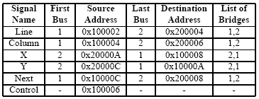
Table 2: Address table for the second mapping example.
6 Conclusions
Rapid and correct-by-construction hardware/software integration is of crucial importance in a platform based design environment for building a flexible system with reusable IPs and CPU cores. In this paper we have presented a methodology for providing automatic hardware/software integration capabilities on multi-processor architectures. The key component of the proposed methodology is a programmatic interface generation tool for automating the generation of the hardware/ software interface mechanisms. The major outcome for designers is the possibility to experiment very quickly with different system architectures without having to perform the tedious and error-prone task of hardware/software integration.
References
[1] M. Lajolo, “IP-Based SOC Design in a C-based design methodology,” in Proc. of IP Based SoC Design 2003, pp. 203–208, Oct. 2003
Related Semiconductor IP
- Ultra-Low-Power LPDDR3/LPDDR2/DDR3L Combo Subsystem
- 1G BASE-T Ethernet Verification IP
- Network-on-Chip (NoC)
- Microsecond Channel (MSC/MSC-Plus) Controller
- 12-bit, 400 MSPS SAR ADC - TSMC 12nm FFC
Related Articles
- Why Interlaken is a great choice for architecting chip to chip communications in AI chips
- From I2C to I3C: Evolution of Two-Wire Communication in Embedded Systems
- High-Speed Serial fully digital interface between WLAN RF and BB chips
- Hardware/Software Partitioning and Interface Synthesis in Networks On Chip
Latest Articles
- Extending and Accelerating Inner Product Masking with Fault Detection via Instruction Set Extension
- ioPUF+: A PUF Based on I/O Pull-Up/Down Resistors for Secret Key Generation in IoT Nodes
- In-Situ Encryption of Single-Transistor Nonvolatile Memories without Density Loss
- David vs. Goliath: Can Small Models Win Big with Agentic AI in Hardware Design?
- RoMe: Row Granularity Access Memory System for Large Language Models