High Performance Connectivity IP -- Avoiding Pitfalls When Selecting An IP Vendor
Mountain View, California USA
Abstract:
The demand for connectivity IP for high speed serial busses such as USB 2.0, PCI Express®, SATA, DDR2 and HDMI is increasing as standard interfaces in applications such as single chip recordable DVD CODEC’s and MP3 players. In order to stretch battery life of these chips, the semiconductor technologies require ultra-low power derivatives of high-performance logic manufacturing processes, enabling production of very low-power chips for these mobile platforms and small-form factor devices. Today many of these chips are manufactured in 90 nm, and the ramp for 65 nm design starts has been more aggressive than expected. 45 nm is following close behind, with early versions of design rules and process parameters already available. Since connectivity IP requires both a digital controller (MAC) and mixed-signal circuitry (PHY), the challenge is to meet analog performance in a technology that has been targeted for densely packed digital logic.
IP is the critical enabler to meet the time to market demands for these SoC’s and an industry of IP providers has mushroomed to service this demand. The key question for the SoC developer, and the goal of this paper, is to highlight the importance of selecting the right IP vendor – how to avoid the pitfalls.
In this paper, we will discuss how to select a third party IP vendor, how to verify third party IP, and some of the gotcha's when integrating third party IP, with a special focus on the SerDes-based PHYs for PCI Express and SATA as well as PHYs for USB and DDR2. In addition, we will discuss the impact of 65 nm and 45 nm process effects on yield, we will review the advantages and disadvantages of moving to serial links, we will propose complete vertical integrated solutions, and we will present production testing techniques.
As the number of third party IP vendors increase, the quality of the IP available varies. This paper discusses IP selection criteria to ensure that the right choices are made.
Figure 1 highlights the essential elements of IP selection, in terms of functional correctness, integration, usability and support.
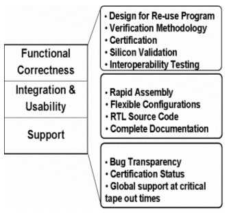
Figure 1 Essential elements of IP Selection
Obviously, the IP must be correct functionally, but other factors are important such as ease of integration and support by experienced protocol experts – with design teams located world-wide, the IP vendor must be able to provide this support round-the-clock, every day.
1.0 The Gotcha’s – The Ten Questions
Figure 1 described a high-level view of IP vendor selection, but due to the complex nature of connectivity IP, further investigation is needed. The following are the ten most important considerations:
-
How mature is the IP being sold? Has this IP taped-out in silicon? What process and foundry?
-
Or, if the IP is mature, how many customers are shipping ICs using this IP?
-
Does the IP design team have high-speed design experience using deep sub-micron CMOS technologies with low supply voltages?
-
Are there any customers that have used or are now using this IP? If so, can you contact them for reference and to find out if there were any serious problems with the IP?
-
How was this IP verified? Has it been certified by any independent standards or compliance body?
-
What are the current errata? Is there a plan to fix the current bugs? What is the vendor’s willingness to share such errata?
-
What is the vendor’s track record in the industry?
-
What level of support is the IP vendor willing to provide? Is the vendor willing to offer services to customize the IP for the application?
-
What level of integration support is needed? Are there any special process options required, for example deep NWELL, thick metal for inductors, MiM capacitors or varactors?
-
Has the IP been tested for ESD and latch-up robustness? Are ESD guidelines provided?
Unless the IP being purchased is mature, it may contain bugs. Due to the increasingly complex nature of IP, before any purchase is made, the first step in doing due diligence on third party IP is to determine the impact of the current bugs (and any other errata) on the intended application. Some bugs may only be present when specific features or configurations are enabled. If the bugs do affect the intended application, it is important to get a written commitment and schedule for their correction.
Figure 2 shows the seven layer OSI model. For connectivity IP, this is divided into levels L1 to L4. Ideally, an interface standard (e.g., USB and PCI Express) IP vendor should provide a complete solution including all of these, essentially circumventing interoperability issues.
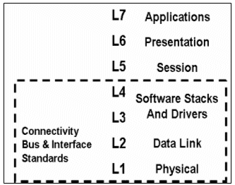
Figure 2 Seven layer OSI model
The second step in the process is to determine how thoroughly the IP was verified. For mature IP (which has undergone multiple successful tape-outs), this effort is minimal. However, for new or emerging IP, the certification and verification effort can be challenging. This effort is usually underestimated by the SoC implementer, and in some cases ignored by the IP vendor. The key is to ensure that the IP has gone through a certification process, for example with PCIe SIG.
The third step is to get written commitment from the vendor on issues that you may find during product development and IP integration.
The next section discusses the above challenges in the context of the commonly used and emerging IP.
2.0 High Speed Serial Links
Recently, high-speed serial links have become increasingly common place in the industry. There are a number of advantages to using high-speed serial links instead of source-synchronous parallel I/O currently deployed. Because of their advantages, the industry will be moving toward high-speed serial links for those applications where performance, footprint, and cost are paramount. The popular protocols are the SerDes based (serializer-deserializer) PHY’s for PCI Express and SATA. Figure 3 clearly shows the advantage of using the serial based approach compared to the parallel cable.
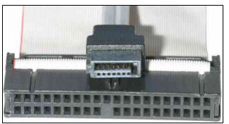
Figure 3 ATA cable (below) and SATA cable
2.1 High Speed Serial Link Advantages
The following summarizes the advantages of serial links.
-
No setup/hold requirements on data lines. Because both data and clock are embedded in the same differential pair, this simplifies routing on a printed circuit board. For parallel I/O, the clock and data pins have to be routed so that all data lanes meet the setup and hold requirements of the source synchronous clock.
-
Less pins required. To achieve the same performance as a single PCI Express link, a comparable parallel interface would need to run at 250 MHz with 8 data and 1 clock pins compared to just 2 pins for a serial link.
-
Greater bandwidth per pin. This minimized the number of pins required and number of traces on the printed circuit board (PCB). Minimizing I/O allows the use of a cheaper package with a smaller footprint. Using a cheaper package lowers overall ASIC cost. Moreover, by using a smaller footprint, the printed circuit board cost is minimized as well.
-
High-speed. A single PCI Express link provides 2.5 Gbps bandwidth while even the high-speed Pentium 4 Front Side Bus (FSB) runs at a maximum of only 1066 MHz. (Future PCI Express device will support 5 Gbps bandwidth)
2.2 High Speed Serial Link Disadvantages
There are some disadvantages and these should be discussed with the IP vendor.
- Debug is more difficult since a standard logic analyzer cannot easily hook up to a high-speed serial link. Expensive oscilloscopes may be needed to debug signal integrity issues.
- Layout of a serial link is complex due to the need to observe routing and termination requirements for the differential pair.
2.3 Choosing Serial Link IP
As with any new technology, the trade-offs between developing the high-speed serial link interface internally or licensing the IP through a third party need to be thoroughly examined.
The high speed serial link consists of two layers: the physical layer (PHY) and the media-access layer (MAC). The PHY is responsible for merging slow incoming data (16 bits at 125 MHz for PCI Express) and clock (125 MHz for PCI Express) and generating two differential high-speed outputs (2.5 Gbps). The PHY is also responsible for decoding the incoming high-speed serial data stream. The MAC handles all high-level functionality, such as flow control, transaction generation, routing, etc. In PCI Express and SATA, the MAC layer includes the transaction layer and the data link layer.
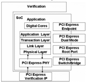
Figure 4 PCI Express, complete solution
Since the PCI Express and SATA PHY’s are complex (involving high-speed analog/mixed-signal design), it is usually licensed from a third party. Few companies are capable of developing the PHY internally or in sufficient time.
The MAC can either be developed internally or licensed as well. This will largely depend on the time to market requirements, availability if suitable IP, and verification requirements. For PCI Express and SATA, with strict requirements in compatibility, verification, and testing, the development time for the MAC layer can be quite long. For this reason, licensing the MAC as well as the PHY makes sense.
When licensing both the PHY and MAC layers from the same third party, the two layers should have been tested together. It is important to know what configurations were tested together and what methods of verification were utilized. Figure 4 PCI Express, complete solution shows the PCI Express complete solution with various configurations of MAC that are available and also the verification IP.
If the two layers are licensed from two different vendors, then the verification challenge is much greater. For example, in PCI Express, the majority of PHY and MAC layers communicate to each other over the PIPE interface (as defined by Intel). Although PIPE is a standard, it can be interpreted differently by different vendors. In addition, low-power functionality is not very clearly specified. These issues can lead to bugs. Thus, it is very important to understand not only the PIPE interface spec – but the implementation assumptions made by both vendors.
3.0 My Chip Needs USB 2.0
Almost all mobile devices require USB functionality and in addition to the points made above the target for USB is to be low in power and area. Therefore the IP vendor must provide a core that is competitive in area and power without sacrificing performance.
Significant area reduction can be achieved through a combination of architectural and implementation optimizations. For example, the PLL/DLL architecture should be targeted to support the 12/24/48 MHz reference frequencies with 480 Mbs output. Also products requiring USB IP tend to follow the aggressive feature size reductions and therefore the PHY should be floor-planned in such a way that as the digital block scales with the smaller process geometries, allowing the overall macro area to shrink -- this is not always the case with analog/mixed-signal designs.
Another important consideration is the pin count design – low pin count is a major advantage in terms of enabling the use of lower-cost packaging. The need for fewer pins also reduces the cost of production test, as well as considerably easing SoC integration.
With the transition from 90 nm to 65 nm and 45 nm process geometries, yield has assumed a much higher priority. With USB, chip yield is linked to the performance of key specification parameters, such as PLL jitter performance and band-gap variation, as well as being dependent on chip area. A lower chip yield, even by as little as two or three per cent, can cause manufacturing cost increases which may overwhelm any savings that are achieved with a smaller die area.
4.0 Why Should I Ask For A Complete DDR2 Memory Interface Solution?
The benefits of high performance DDR2 SDRAM memories require systems-on-chip (SoC) interface designers to approach memory subsystem integration with attention to detail. As data rates have progressively increased from DDR2 400, DDR2 533, DDR2 667, and now DDR2 800, the complexities associated with the timing and signal integrity of the memory interface has become increasing difficult.
Migrating from 400 Mbps to 800 Mbps DDR2 requires additional engineering effort. Ideally, this migration was planned for when the 400 Mbps application was first implemented. For DDR signaling, increasing frequency reduces total bit time from 2.5 ns to 1.25 ns. This bit time is then evenly divided into a setup-and-hold budget of 625 ps each. Source synchronous timing depends on the uncertainty of the placement of the DQ data edge relative to the DQS strobe edge. Any skew, jitter or uncertainty component will erode the setup and hold margins.
Total timing is composed of three budgets: Transmitter, Interconnect, and Receiver. Nominally, each of these three budgets account for about 33% of the total timing budget. JEDEC managed to scale down the DRAM contributors to the transmitter budget (during Reads) and the receiver budget (during Writes) accordingly with the increase in frequency. Unfortunately, the scaling is not applied proportional to the bit period as data rates increase. For example, the uncertainty of when the DRAM will generate DQS relative to CK is +/- tDQSCK. For DDR2 400, this is +/- 500 ps, or 40% of the 2500 ps bit time. For DDR2 800, this is +/- 350ps, or 56% of the 1250 ps bit time. Assume also, that the system designer planned for this migration and specified the controller, PHY, and I/O cell to meet 800 Mbps timing at the beginning of the project. The remaining timing budget is consumed by the interconnect between the PHY and the DRAM. Three items in particular in the interconnect budget need to be addressed.
4.1 PCB and Package Skew
The electrical length differences between the DQS and the DQ of a particular byte must be reduced to meet the now reduced timing budget. Where a 35 ps skew budget may have been adequate for 400 Mbps, less than 20 ps may be required at 800 Mbps.
4.2 Inter-Symbol Interference (ISI)
This effect is the overlap of random signal bits at the receiver. ISI is exacerbated by capacitive loading of the net and frequency dependent losses in the channel routing. The impact is to increase the data-dependent jitter at the receiver thresholds and reduce the minimum amplitude of the received signal. Both of these effects can be captured in eye-patterns. When the bit rate doubles, these effects will increase since the signal now has 50% less time to reach the required threshold levels. DDR2 has lower AC thresholds at 800 Mbps that addresses the amplitude issue; however, increased data-dependent jitter will still be a problem.
Fortunately, the capacitive loading can be reduced by decreasing the number of ranks of memory of each DQ and DQS, consequently reducing the roll-off of the received signal and reducing ISI. The PCB losses can be reduced by shortening the overall route length, using a lower loss dielectric material and/ or increasing the trace width (watch out for crosstalk).
4.3 SSO pushout
During write operations, the DQS is launched 90 degrees out of phase with the eight DQ signals of the byte. When the 8 DQ lines toggle simultaneously, the resulting current draw through the package wire inductance may cause the power rail to collapse, resulting in a delay of the output of the DQ signals. This “push out” will subtract from the available set up time budget. If nothing is done, when the bit rate doubles, the percentage of the budget occupied by SSO push out will also double. To reduce the contribution of SSO, the package wire inductance must be reduced. This can be done by switching from bond wire to flip chip or increasing the number of power/ground pairs in the interface. Other less effective measures would be using double bonds on power and ground, or adding decoupling. Decoupling is most effective when on-die. Decoupling can also be placed close to the die on the pad ring, within the package or surface-mounted to the package. Adding capacitance on the PCB will likely have too much effective inductance to efficiently decouple high-frequency power/ground noise. Any of these solutions increase the cost; therefore, the architect should plan for 800 Mbps operation from the beginning.
Planning is the key. When designing for 400 Mbps, anticipate what will be required to get to 800 Mbps and include it on the front end.
To summarize there are two options:
Customer assembled kit – requires assembly
- Individual I/O, DLL, PLL’s and glue logic
- System performance uncertainty
- High-speed logic/system integrator required
Fully-assembled DDR2 memory PHY macro
- Built-in margin in the design
- Increased certainty of system performance
- Reduce risk and development time
- High speed logic/system integrator not required
In today’s deep sub-micron technologies the following effects impact yield and must be eliminated.
-
STI – Shallow trench isolation - This is a fabrication method used to isolate active areas and can cause currents to be different from simulation and it depends on transistor location.
-
NBTI – Negative bias thermal instability - degrades PMOS devices progressively over time ultimately by an increase in the threshold voltage and reduction in mobility due to negative gate bias and/or higher temperatures usually around 100+C. The net effect is that the PMOS current drive is degraded over time and this can induce timing failures in digital circuits.
-
Matched devices, like current mirrors and differential pairs, which are asymmetrically stressed will have an additional mismatch component, in addition to mismatch from processing variations, causing additional performance degradation to the system.
-
HCI – hot carrier injection - degrades the performance of NMOS devices in a similar way but through a different physical mechanism to NBTI. Unlike NBTI, HCI is a function of the electric field across the channel (i.e. from drain to source) whereas NBTI degradation is a function of the field across the oxide.
-
Circuit layout must be able to accommodate well proximity effects.
-
Electro-migration checks for potential short conditions must be made. This can occur on dense arrays of conducting thin-film metallic conductors, and over time, high current densities cause these conductors to fail causing metal separation.
-
Also, there should be checks for adequate metal widths and checks for metal / MOS / POLY / VIA / contacts.
These effects do have a serious impact on the design of the analog/mixed-signal portions of the connectivity IP and the vendor must have deep expertise in understanding these effects.
6.0 IP Testing & Verification
Thorough validation of IP involves two phases: pre-silicon and post-silicon verification. For pre-silicon verification, the following steps may be necessary:
-
Vendor IP verification - run vendor’s provided test vectors to verify the IP. This is usually done at Verilog/VHDL RTL level and verifies that the IP delivered is functional. Synthesis can be done at this time as well, to check for any synthesis issues.
-
Vendor IP certification – using in-house or externally purchased test vectors and test benches, to verify the quality of the IP purchased by running a test suite. This independent certification may find issues on the IP itself that may have been missed by vendor’s own test vectors. This is especially important for technologies which are not mature or for IP with limited silicon tape-outs.
-
Vendor IP integration – using in-house vectors, verify the usage model of the IP. Although the IP may be defect-free, it may be hooked up incorrectly or used in ways for which it was not intended. Consequently, it is very important to have sufficient test cases and test benches to thoroughly exercise all the usage modes of the third party IP.
-
FPGA verification platform – if possible, map the entire (or subset) design to an FPGA and verify the IP on a development board. Many FPGAs currently exist which support high speed serial links (Xilinx). In addition, there are off the shelf development platforms available (Dini) which can be purchased to speed up this development. This platform can be used to verify the MAC layer and speed-up software driver development.
-
Hardware acceleration platform – if access to hardware acceleration is available, it may be quite beneficial to verify the design and get a head start on software driver development. Bugs are much easier to identify and correct in a hardware acceleration environment than in a FPGA environment.
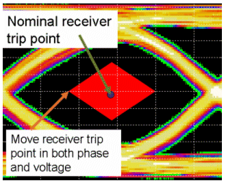
Figure 5 The received eye for PCI Express - On board diagnostics
For post-silicon verification, the following steps are necessary:
-
Serial I/O testing – for high-speed serial links, (including USB and DDR2) special testing equipment, including high-speed oscilloscopes may be necessary to verify that the quality of the PHY electrical signaling. These will be able to measure the eye-diagram, jitter, and other electrical parameters necessary for serial link certification. Having visibility into the received eye as shown in Figure 5 is a very useful capability to show the link performance. This eye-diagram was taken via the JTAG port and viewed on a PC – without using any test equipment.
-
MAC Verification – to thoroughly exercise the media access layer, a number of stand-alone platforms are available from Catalyst and Agere. These platforms send specific test patterns to the device under test (DUT) and expect a specific response. These can be used to identify MAC compatibility and certification issues, in the example of PCI Express, before going to PCI-SIG or some other certification body.
-
The SoC designers do not design the IP and therefore cannot add test features. If they cannot simulate it with a test bench, they cannot test it.
-
SoC test engineers usually have vectors they stream in/out from simulation. All analog tests have to be hand coded.
-
Test engineers have to devise tests to get acceptable analog fault coverage. The designers do not know much about the analog portion of the IP.
-
Most analog tests require external hardware to properly test. Setting up this hardware takes time.
The first time test vectors/code are tested on real silicon is when the SoC comes back.
So how does the test engineer incorporate the PCI Express compliance eye-mask into the ATE without changing the signal? He certainly cannot hang a high speed tester on each pin. The test engineer’s concern is that with the simple pass/fail test of the external loop-back approach he will not know how much margin he has – chips that pass the loop back test that are marginal may fail over time when subjected to real world conditions. Referring again to Figure 5, using voltage and phase margining the link can be reliably tested in a production test environment. These limits are set by simple input and compare vectors that are provided with the IP. A comparison of this approach with the conventional method is outlined in Table 1.
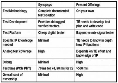
Table 1 High speed SerDes testing comparison
8.0 Conclusions
This paper reviewed in detail the important considerations for selecting an IP vendor. The key considerations can be summarized as:
-
In order to be successful the IP vendor must have a track record of customer wins and silicon success.
-
The vendor should offer a complete solution: MAC, PHY and verification IP. These should interoperate and have gone through compliance testing and plug-fests.
-
The IP design team must be experienced in the connectivity protocols and have the analog/mixed signal design expertise to design in the latest deep sub-micron technologies.
-
The IP vendor supporting the interconnect demands of today must also have a roadmap for future standards and broad coverage of fabrication technologies.
-
World-wide support must be available during tape-out and after the SoC comes back.
Navraj Nandra is Director, Marketing Mixed-Signal IP at Synopsys.
Acknowledgements
Contributions to this paper were made by Gervais Fong, David Wallace, Joe Guiliano, Bob Lefferts (Synopsys) Boris Litinsky (Juniper Networks)
Related Semiconductor IP
- 64G SerDes
- 112G SerDes USR & XSR
- Extended Long-Reach (XLR) Multi Standard SerDes (MSS) IP
- 4.25 Gbps Multi-Standard SerDes
- 1-56Gbps Serdes - 7nm (Multi-reference Clock)
Related White Papers
- High Speed Serial Interconnects - What to Look for When Selecting an IP Vendor
- Building high performance interrupt responses into an embedded SoC design
- Plug-n-play UVM Environment for Verification of Interrupts in an IP
- When Developing New Silicon IP, Is First Pass Success Possible?
Latest White Papers
- Ramping Up Open-Source RISC-V Cores: Assessing the Energy Efficiency of Superscalar, Out-of-Order Execution
- Transition Fixes in 3nm Multi-Voltage SoC Design
- CXL Topology-Aware and Expander-Driven Prefetching: Unlocking SSD Performance
- Breaking the Memory Bandwidth Boundary. GDDR7 IP Design Challenges & Solutions
- Automating NoC Design to Tackle Rising SoC Complexity