Transition Fixes in 3nm Multi-Voltage SoC Design
By Rahul Parmar and Mayursinh Vansadiya, eInfochips
Abstract
As the semiconductor industry shrinks toward lower technology nodes (3nm and below), the integration of a multi-voltage design presents both opportunity and challenges in today’s world where power optimization is critical. However, these designs introduce complex issues related to transition across different voltage domains present in the design. The transition issue is one of the significant concerns that directly impacts the power, performance, and area (PPA) of the chip. This white paper explores what transition is, what are the root causes of transition in a multi-voltage design and its impact on timing and signal integrity. It also proposes robust and efficient practical real-world solutions to address and solve these challenges in such a way that it does not impact the design while meeting the chip requirements. By systematically examining these complexities related to multi-voltage, we present comprehensive, efficient and practical solutions based on real-world implementation.
Introduction
In the pursuit of creating faster and more energy-efficient System on Chips (SoC), the semiconductor industry is leading toward innovative multi-voltage design strategies for power saving. However, multi-voltage designs come with their own problems related to transition. With the continuous scaling of semiconductor technology to lower technology nodes, the 3nm era introduces new hurdles for Application Specific Integrated Circuit (ASIC) physical design engineers in optimizing power within multi-voltage designs.
As low power designs are very complex nowadays in lower technology nodes to achieve better power efficient chip, multi-voltage design is power optimization techniques used in modern ASIC design. Operating different sections of a design at different voltage levels enables substantial power savings without compromising performance targets. As a result, new transition related concerns may appear in different voltage domains.
Transition issues in multi-voltage design have become increasingly crucial, impacting timing, power, and overall design reliability. These factors make it difficult to achieve optimal power, timing, and performance trade-offs. This white paper aims to travel through the complexities of transition issues and its consequences in multi-voltage designs. Furthermore, it shows the practical approaches and successful techniques implemented and tested in real-world projects to address these problems, which lead to efficient chip performance.
What is transition or slew?
Transition or slew is the delay taken by a signal to rise from logic “0” to “1” or to fall from logic “1” to “0”. Transition is calculated from 20% to 90% of the maximum value during rising edge and from 90% to 20% of the maximum value during falling edge. In other words, it is time or delay taken by the pin to change its current state.
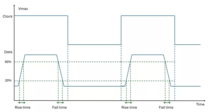
Fig 1. Transition Diagram
There are two types of transitions that can occur in a design. Let’s go through them briefly.
Clock transition: Clock transition refers to the slew when the clock propagates through the clock tree. Clock tree switches constantly to ensure all sequential elements receive proper clock. Clock transition directly affects the duty cycle of the clock which affects the timing and performance. As a result, the clock does not propagate properly to the clock pins (characterized in .lib) because of the delay in the rise time or the fall time. That is why clock transition needs to be fixed carefully, especially when the design operates in multi-voltage.
Data transition: Data transition refers to the slew present on functional (non-clock) path. Data transition can lead to inaccurate delays of standard cells (not following timing model characterized in .lib) and can cause setup/hold violations. In a multi-voltage design, data transition becomes even more challenging as level shifters and isolation cells are present in the design. The designers must take care of how voltage domains are created in the design and based on that, decide how to fix the transition issues.
Why do we need to fix transition issues?
In the ASIC design, each standard cell is characterized in a .lib file with a specified maximum input transition for noise, timing, and power modeling. If the actual transition on the input pin exceeds this value, the library model specified in the .lib file becomes invalid, resulting in inaccurate delays during static timing analysis. So, the standard cell does not function how it is supposed to, causing timing degradation leading to functional failure. These violations are critical, particularly in multi-voltage designs where cells are placed in different voltage domains having different load conditions, increasing the transition violation. Therefore, it is essential to fix the transition/slew issues to achieve reliable and predictable chip behavior across all voltage domains.
Transition liberty limit (lib limit)
The liberty limit (lib limit) refers to the upper threshold value of the signal transition. It specifies the maximum transition duration for which the cell timing and power are perfectly characterized. These values are defined in the .lib file for input pin of the standard cell present in the library, either from the foundry or from the vendor. Any actual transition slack exceeding this value leads to unreliable results and can affect chip performance.
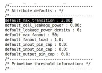
Fig 2. Max Transition Limit in a Standard Cell Library
Figure 2 shows that the default maximum transition value defined in a standard cell library is 2ns and figure 3 is the transition report in which the lib limit for the transition is mentioned. According to the report, the limit set in the .lib file for transition in the analyzed block is 0.3097. It means the input transition for the standard cell library is characterized up to a maximum of 0.3097. Any actual transition slack exceeding this value can affect the timing, power and results might not be accurate.
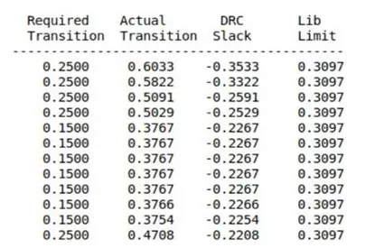
Fig 3. Transition Report with Lib Limit
Why transition issues occur in design?
There are multiple factors why transition issues can occur in a design. Let’s try to understand them in detail.
- Long routing of nets: If the net routing connected to the input or output pin is too long, it can create transition issues. The longer the route, the more delay the net takes while changing its current state. For example, if the routing of any net on layer M6 is >=200 microns, there are possibilities that this net can cause transition issues on the pin because of the long route. The longer the route, the more transition delay occurs on the pin. However, 200 microns is not an ideal length, it can vary.
- Weak drivers: If the driver of the net is weak, it can cause transition issues. Weak drivers are unable to drive long nets effectively, resulting in increased delays during switching activities.
- Fanout: Fanout is another important factor that should be considered. If the driver has a high fanout and is weak, it struggles to drive the multiple loads effectively, potentially leading to transition violations. Consider scenario where the driver has the drive strength of X2 and the fanout is 10, then X2 driver cannot drive this much load easily, causing the transition on the output pin of the driver, affecting the timing.
- Crosstalk: Transition can also occur because of crosstalk. When two nets have a long parallel route and enough track is not present between these two nets then coupling capacitance of aggressor can cause transition issues on the victim net, degrading the timing.
- Routing on lower layers: If most of the net routing is on the lower layer, it can cause transition issues as the lower layer has more resistance compared to the higher layers, eventually causing more delay (Ohm’s law, V=IR).
How to resolve transition issues?
- Buffering the net: If the net routing is long, the designers can break that net by inserting a buffer. Depending on the net’s routing, different scenarios may arise, and the designer must determine the most effective way to break the nets accordingly. Here are the scenarios:
- If the net routing is too long (say > 400 microns), the designer can add a buffer at a repeater distance of 100 or 150 based on the net’s routing. The repeater distance can vary based on how long the net is routed and the designer can decide how much it can help.
- If the net routing is relatively short, the designer can break it in half by inserting a buffer with a buffer insertion ratio of 0.5.
- If there is a requirement for the designer to break the net by adding a buffer at a specific location or coordinate, the designer can provide the coordinates and guide the tool where to add the buffer.
- Upsizing the driver: If a driver is too weak to drive the net, the designer can upsize the driver. Ideally the designer should double the drive strength (from X4 to X8). If the driver is X1 or X2 only, it should be upsized at least X4 depending on the requirement. Another important check is to ensure that the driver's placement location has sufficient space to allow for upsizing. If the driver is placed in a congested area, the designer needs to think of a different approach to solve transition violations and ensure that the area is not an Electromigration and IR drop (EMIR) hotspot.
- Layer promotion to higher layer: If the net’s routing is on the lower layer, the designer can promote these nets to a higher layer based on the track availability to solve the transition issues. Higher layers have lower resistance that results in reduced delay and improved transition.
- Fixing Crosstalk: If crosstalk is present on the net, two methods can be used to fix transition and crosstalk violations simultaneously. Crosstalk can be analyzed using the command report_delay_calculation in a primetime session. The designer can open setup scenario to analyze crosstalk and check report_timing -through <net_name> to check aggressor and victim nets. The designer can check crosstalk by passing the pins of this nets in primetime using command report_delay_calculation -from <cell/OUT> -to <cell/IN> -delta command. <cell/OUT> means output pin of driver and <cell/IN> means input pins of sink.
- Break the net in half by adding a buffer to reduce the coupling capacitance on the victim net, hence improving transition.
- Implement layer promotion and transfer the net routing to a higher layer with enough tracks present. For example, if most of the net routing is on M3 and M4, the designer can direct these nets to M7 and M8 based on the resource availability on these respective layers.
The next section of the paper covers each of these categories in detail - how to analyze these, how to implement them practically, and what precautions to take while fixing these types of violations related to multi-voltage designs without affecting the performance.
Practical approach and methodology to solve transition
After covering the theoretical basics of transition, let's explore a practical approach to analyzing and understanding the methodology to resolve transition issues in a multi-voltage design. Before starting, let’s go through the basics of an isolation cell and level shifter cells that are used in the multi-voltage design.
Isolation cell: Isolation cells are used in the multi voltage design to isolate different voltage areas to ensure proper functionality and signal integrity across different voltage domains. These cells are very useful to minimize the leakage current. When a power domain is turned off, its output signals become undefined (floating or metastable), which can propagate invalid logic states (don't care - X) to different domains present in design. Isolation cells clamp these logic signals to predefined or stable logic states to ensure receiving domains interpret valid logic levels, preventing functional errors or metastability. These cells are inserted at the boundary of the shutdown domains.
Level shifters: These cells are used to shift the voltage levels between voltage domains, ensuring proper signal interpretation across domains. These cells enable communication between two voltage domains ensuring proper data transfer.
To have a theoretical foundation of transition in a multi-voltage design within 3nm technology node, it is vital to bridge the gap between conceptual understanding and practical approach. This section of the paper delves into innovative and targeted strategies employed during the design and implementation phases to address the transition issues effectively.
1- Consider a scenario where the driver and the sink both are on the same voltage domains, but the net routing is going through another voltage domain. It is called voltage hopping. The purple dotted line separates the voltage domains.
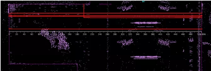
Fig 4. Voltage Hopping (Horizontally)
In figure 4, the red ones are the nets that have transition violations. The drivers of these nets are located on the right side and the sink is placed on the left side. Both are on the same voltage domain, but the routing goes through a different voltage domain. The length of these nets is approximately 510 microns. These violations occur because the nets have long horizontal routing on the lower layer M6. The tool was unable to address and solve the transition issues on its own, because some nets have the X2 and X4 drivers that cannot drive a long net. Another reason was during the ECO flow; the tool somehow set the maximum layer rule of M6 on these nets. To solve this problem, the designer can upsize the driver to X8 or X16 to drive these long nets and reset the lower-layer and upper-layer constraints, applying the minimum layer routing rule M12 on these nets. So, during the route_eco process, the tool starts the routing from M12 or above layers. One thing to consider is that the designer cannot break these nets because there is a different voltage domain in between. If the designer breaks these nets by inserting buffers, the newly added buffers are placed in different domains, failing the Low Power Verification (LPV) check. These are the FC commands to solve the transition issues in voltage hopping:
- To upsize the driver:
size_cell cell_name cell_ref_name_X16
- To reset routing rule and apply user specified min-max layer rule:
set_routing_rule -clear [get_nets <net_name>] ;#resets the routing rule
remove_routes -detail_route -user_route -nets [get_nets <net_name>] ;#removing existing routing of net
set_routing_rule -min_layer_mode "allow_pin_connection" -min_layer_mode_soft_cost "high" -min_routing_layer M12 -max_routing_layer M15 [get_nets <net_name>] ;#set min layer M12 and max layer M15 rule for net
Another scenario in the same category is long vertical routing where the driver is placed in the bottom area and the sink is on top. There was a long vertical routing of approximately 280 microns on M5. Look at figure 5 below:
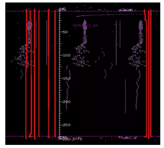
Fig 5. Voltage Hopping (Vertically)
The approach to solve these violations remains the same that addresses the case mentioned above. The designer can upsize the driver and set the minimum layer routing rule. One thing to cross check before applying the minimum layer rule in both cases, is that the designer needs to check resource availability in that area. If tracks are not available on the specified layer, after running route_eco, there is a possibility that new routing may introduce shorts or Design Rule Check (DRC) violations in that area. So, choose the layer in which tracks are available.
2- Consider a case where both the sink and the driver are in the same voltage domain, but their route is long. For these types of nets, the designer needs to break the net to solve transition issues. Refer the figure 6 where nets have long routing of approximately 700 microns. There are three possible methods a designer can use to break nets, depending on their routing. Here are the details of each category:
- If the net routing is long, the designer can break these nets at a repeater distance. The designer can decide the repeater distance based on how long the route is. Here is the FC command to break the net:
add_buffer_on_route -repeater_distance 100 -verbose [get_nets <net_name>] buffer_ref_name
The following command breaks the net at 100 microns using the buffer provided at the end. - If the net routing is in medium range (not too long and not too short), the designer can break that net in half by providing a ratio of 0.5. Here is the FC command to do so:
add_buffer_on_route -repeater_distance_length_ratio 0.5 -verbose [get_nets <net_name>] buffer_ref_name - If there is a case where the designer needs to break the net at a certain location or coordinate, then here is the FC command to do so:
add_buffer_on_route -location {x1 y1 layer_name} -verbose [get_nets <net_name>] buffer_ref_name
In the above command, the designer needs to provide the X coordinate, Y coordinate, and the layer on which it needs to break the net. For example, {1500 1200 M10}.
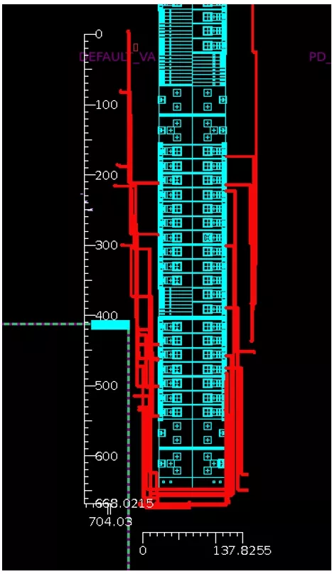
Fig 6. To Break the Net
In all three cases, the designer can also provide the prefix of the newly added cells and the net using the following switches: -net_prefix <user_prefix> and -cell_prefix <user_prefix>. These prefixes can help a lot if the designer needs to discard the changes in case the fixes don’t work or analyze afterwards. These methods are useful where multi-voltage is not present.
3- Consider a case where the sink and the driver are on a different voltage domain. It is called cross domain nets. These types of nets are quite challenging to solve. For these types of nets, first the designer needs to check which layer the routing is done in. If the routing is on the lower layer, the designer can promote it to a higher layer, which can solve the issue. If the net is already on a higher layer, the designer needs to provide the location explicitly where to break the net and needs to change the voltage domain of the newly added buffers. Here is the FC command to set the voltage domain:
create_power_domain <voltage_domain_name> -elements <cell_list> -update
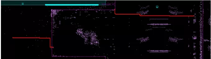
Fig 7. Cross Domain Nets
Another way is that the designer can move the sink near to the driver or vice versa and set the physical status of the sink/driver to legalize_only. So, during route_eco, the tool legalizes these cells and snaps them to the finfet grid. By doing this, the routing between the sink and the drive is reduced. After moving the sink or driver, the designer must also check how far the net connected to the input pin of the moved cell extends. If the net is far, the designer cannot move these cells as it can create an issue in the next set of runs.
4- Consider a case where the driver has a high fanout and the driver is placed in congested area. In this case, buffer insertion or driver upsizing does not help as it becomes more congested and can cause IR issue in that congested area. Refer figure 8.
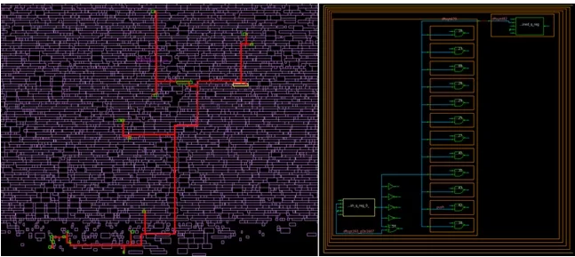
Fig 8. High fanout net at congested area
The yellow one is the driver, and the green ones are the fanout/loads. For better understanding, schematic is on the right to understand the connection between them. In this case, the designer needs to do load splitting by adding a buffer and dividing the load. Here is the FC command to do load split:
split_fanout -net <net_name> -net_prefix <user_prefix> -cell_prefix <user_prefix> -loads {cell1/IN, cell2/IN, …, celln/IN} -lib_cell buffer_ref_name
In –loads switch, the designer must provide the input pins of all the cells for which load splitting is required. So, the tool adds one buffer and connects to all loads. By doing this, the number of loads on the driver reduces and the newly added buffer helps to drive the rest of the loads.
5- Consider a case where the driver is a macro. In this condition, the designer must check the net routing. Based on the routing of that net, the designer can decide which solution to choose, layer promotion or buffering the net. If routing is on the lower layer, promote it to a higher layer as explained in section A.b. If the net is long and on a higher layer, continue with breaking the net by inserting a buffer based on the categories covered in section B. Ensure that after inserting the buffers, the power domain of the newly added buffer should be the same as the power domain of the macro, otherwise it can fail LPV. So, create a power domain same as the macro using the command mentioned in section C to make sure it passes LPV.
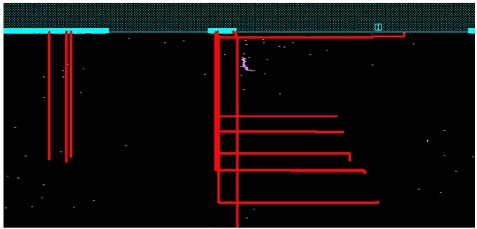
Fig 9. Driver is a macro
6- Consider the case where the driver is an isolation cell and the sink is on a different voltage domain. Refer figure 10 below. The isolation cell is placed in a different domain and the sink is in another domain. Also, the driver is far away from the sink.
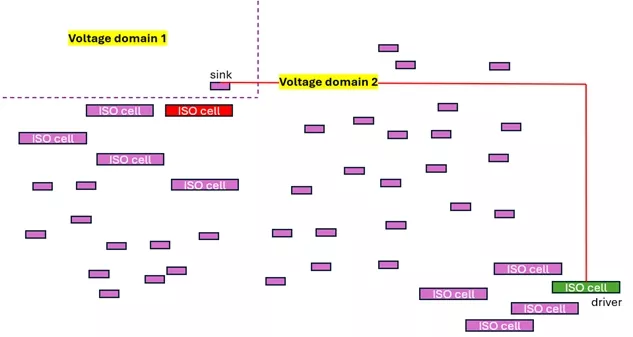
Fig 10. Isolation cell reallocation (before)
To solve this problem, first locate any isolation cell that is near to sink (highlighted in red). Then move the driver (highlighted in green) near to that isolation cell (highlighted in red) and set physical status legalize_only on that isolation cell. Then disconnect the enable pin EN of the driver (highlighted in green) and connect that EN pin to the isolation cell (highlighted in red) that is near the sink. The advantage of this approach is that it reduces the routing length and the distance between the driver and the sink that helps resolve transition issues. These are the series of commands to do this:
set cell_EN_pin [get_pins <cell_name_green>/EN]
set cell1_EN_pin [get_pins <cell_name_red>/EN]
disconnect_net [get_nets -of $cell_EN_pin] [get_pins $cell_EN_pin]
connect_net [get_nets -of $cell1_EN_pin] [get_pins $cell_EN_pin]
Generally, designers should follow the guideline that all the isolation cells should be placed as close as possible to the boundary of the switchable domain to avoid this type of violation in design. Once isolation reallocation is done, this is how the new connection looks like. Refer figure 11.
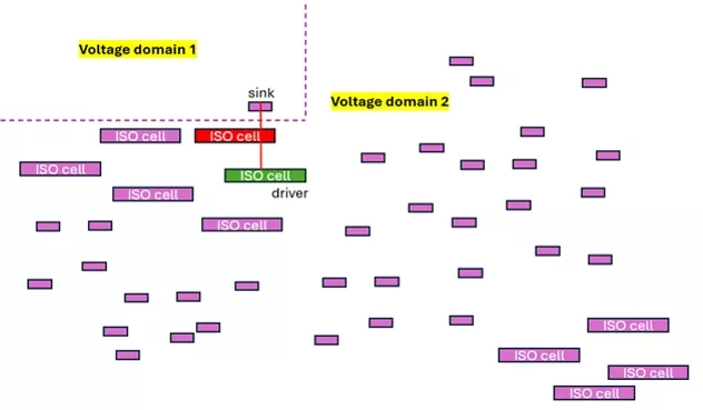
Fig 11. Isolation cell reallocation (after)
7- Consider a case where transition occurs because of crosstalk. In our design, some of the nets had crosstalk as nets had long parallel routing on the M14 layer and area in M14 was congested. Refer figure 12.
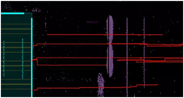
Fig 12. Crosstalk using M16 segment (before)
To solve this violation, create an M16 shape in such a way that it is near to the sink and the driver. Generally, signal routing is allowed up to the M15 layer and only PG routing was present on M16 and M17. So, there were plenty of resources available at M16 for signal routing. By creating shapes like this, crosstalk can be avoided which eventually helps in fixing the transition. There are three ways to do this:
- Provide the minimum layer routing rule M16 (discussed in section A.b) on those nets.
- Do manual routing of the net on M16 by pressing SHIFT+R and route the net from sink to driver by keeping some distance away from them for tail routing. Once pressed SHIFT+R, select the H and V layer, turn on snaping and choose option user_route in shape use section. Because the tool will not touch any net that has the attribute user_route. So, during route_eco, the net does not get affected by it.
- The designer can create shape using FC command by providing bbox and layer. To create a new shape, use the following command:
remove_routes -user_route -detail_route -nets [get_nets <net_name>]
create_shape -shape_type path -layer M16 -shape_use user_route -net [get_nets <net_name>] -boundary “{{llx lly} {urx ury}}"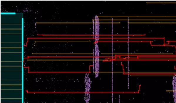
Fig 12. Crosstalk using M16 segment (after)
Once the M16 segmentation is done, this is how the new routing looks like. Refer figure 12.
These are the major approaches that a designer can use to analyze and resolve transition issues by keeping different voltage domains in consideration.
Conclusion
Addressing transition issues in multi-voltage designs at the 3nm technology node is a challenge in itself, crucial for ensuring robust and power-efficient designs. This paper has completed the bridge between theoretical understanding and real-world practical approaches, offering the root cause of transition and presenting practical, proven solutions to meet the challenges without any degradation. By implementing these strategies, designers can ensure cells are functioning properly characterized in .lib, achieve PPA guidelines, maintain signal integrity across voltage domains, and maintain the clock quality without affecting power. As the semiconductor field is evolving, embracing such comprehensive methodologies is essential for successful completion of the SoC.
About authors

Rahul Parmar is working as an ASIC Physical Design Engineer at eInfochips. He holds the Bachelor of Technology (B.Tech) degree in Electronics and Communication from Dharmsinh Desai University (DDU). With three years of experience in the semiconductor industry, he has successfully completed a tape-out of a 3nm project.

Mayursinh Vansadiya has 12 years of experience in physical design and has been working as a Senior Tech Lead Engineer at eInfochips for six plus years. Prior to this, he worked at Open-Silicon Pvt. Ltd. He has contributed to projects across various technology nodes, including 3nm, 16nm, 22nm, 28nm, and 40nm, with expertise in physical design and static timing analysis. He holds a Master's degree in VLSI and Embedded Systems from DA-IICT, Gandhinagar, Gujarat.
Related Semiconductor IP
- NPU IP Core for Mobile
- NPU IP Core for Edge
- Specialized Video Processing NPU IP
- HYPERBUS™ Memory Controller
- AV1 Video Encoder IP
Related White Papers
- EDA in the Cloud Will be Key to Rapid Innovative SoC Design
- Low Power Design in SoC Using Arm IP
- How to manage changing IP in an evolving SoC design
- Integrating VESA DSC and MIPI DSI in a System-on-Chip (SoC): Addressing Design Challenges and Leveraging Arasan IP Portfolio
Latest White Papers
- Transition Fixes in 3nm Multi-Voltage SoC Design
- CXL Topology-Aware and Expander-Driven Prefetching: Unlocking SSD Performance
- Breaking the Memory Bandwidth Boundary. GDDR7 IP Design Challenges & Solutions
- Automating NoC Design to Tackle Rising SoC Complexity
- Memory Prefetching Evaluation of Scientific Applications on a Modern HPC Arm-Based Processor