"Chip Level IP" for low power single chip wireless transceivers
by Colin Faulkner, Jennic
Sheffield, UK
Abstract :
The development of wireless standards designed for low cost, low power transmission of data has led to the commercial availability of single chip devices to address the smallest, lowest cost applications with a low board level design and cost overhead. Examples of this approach include the plethora of devices addressing the Bluetooth market, and a more limited range covering the proprietary low power wireless applications. Correspondingly, a range of IP blocks are available from a number of vendors, addressing the main functions required by these standards. However, these typically cover just the key blocks required, and have not fully followed the trend for single chip solutions. This paper presents an argument for the development of "Chip level IP" for single chip solutions for low power wireless systems, with particular reference to the IEEE802.15.4 standard. The standalone IP needed for such a system is described, along with the requirements for typical single chip designs. The issues involved in the integration of the basic IP to form a single chip design which forms the "Chip level IP" for this standard are discussed in detail.
"CHIP LEVEL IP" FOR LOW POWER SINGLE CHIP WIRELESS TRANSCEIVERS
The concept of the single chip wireless transciever is becoming commonplace, largely due to the success of the Bluetooth device manufacturers. From the early "Single chip" designs which required many peripheral passive and active components in order to operate correctly, a range of highly integrated devices have emerged which provide a true single chip solution for a number of high volume applications.
For this market, there are a diverse range of commercially available IP offerings, ranging from individual RF building blocks (LNA, VCO etc) through radio system designs (RF to baseband conversion) to stand-alone protocol stacks and baseband designs. However, this approach only offers a partial solution to companies wishing to facilitate the design of their own Single Chip Transceiver ICs by taking advantage of IP. A substantial amount of effort is still required to produce a competitive solution from the individual IP blocks available and this may not be commercially viable, particularly where the production volumes for a particular design are lower. An alternative approach, particularly where the requirement is to address a product defined by international standards, is to generate “Chip Level IP”. This needs to solve all of the integration problems for the chip design whilst simultaneously leaving some flexibility for customisation to allow end customers to offer differentiated products.
There are a number of emerging standards which will benefit from the availability of IP supporting them. One example is the recent IEEE802.15.4 low power wireless PHY/MAC standard which will be used by applications in the emerging ZigBee arena for low power wireless systems. This standard offers low data rate communications through a protocol which allows systems to operate with very large numbers of nodes and at very low duty cycles, allowing them to achieve very long battery life. This makes it ideal for applications such as industrial sensors and home or factory automation. A good example is the wireless light switch, where duty cycles are extremely low indeed, yet there is also a requirement for low latency and battery life of several months, or years. The 802.15.4 standard provides for latency of less than 30ms for such a device, enabling fast responses with the possibility of very low duty cycles. The availability of this standard allows standards based solutions, with the consequent benefits of interworking and security, to be adopted in place of the incumbent proprietary solutions which currently address these markets,.
IEEE802.15.4 provides for two different PHY layers, one operating in the 868MHz (in Europe) or 902-928MHz (in the USA) bands and using BPSK modulation, and one in the worldwide 2.4-2.5GHz ISM band which uses Offset QPSK modulation. The examples in this paper relate to the latter frequency band. The standard provides 16 available channels, spaced at 5MHz intervals across the band. The raw data at 250kb/s is encoded using a robust modulation scheme, transmitting one of 16 nearly orthogonal 32 chip sequences to represent 4 bits of actual data, giving, an on air chip rate of 2Mc/s. The on-air modulation scheme used is Offset QPSK, that is, QPSK with the I and Q channels offset by half a symbol. This ensures that transmitted changes result only in phase change, with minimal amplitude variations. The chipping is filtered using a half sine pulse. This scheme is extremely robust, providing a degree of protection against interferers, contributing to low power consumption by minimising any retransmission of failed packets. Further robustness is added by the use of CSMA/CA techniques to establish that the channel is clear before transmission, and the optional use of a beaconing system to allocate timeslots for transmission. Further features of the protocol are the inclusion of AES encryption, providing a high degree of security where required, and 64 bit addressing, effectively providing for an unlimited number of nodes in a given network. A more detailed treatment of the standard can be found in Ref. 1.
To support wireless standards like this, 4 major pieces of IP are required - the Radio, the baseband Modem functionality, Baseband MAC hardware and the protocol stack. These are commonly offered as individual pieces of the jigsaw. However, a key element is often missing and regularly underestimated - the remaining engineering processes required to integrate the IP, and any other functionality needed, into a commercially viable IC. Furthermore, careful consideration of the requirements for, say, power saving, can have a significant influence on the design of the system as a whole. The resolution of this conundrum is for the IP provider to take the designs one step further, and produce a "reference design" which is both a demonstration of the performance of the individual pieces of IP and a ready made design that can be readily taken into production with relatively minor modifications.
We shall discuss the individual IP blocks briefly and consider how they are integrated to produce a single chip solution. As IP blocks, the generic requirements are that the designs are robust, will be tolerant of process porting and provide excellent performance with low power consumption.
The Radio System – Figure 1, is required to translate between the 2.4GHz on air signals and the baseband signals that can be handled by the subsequent signal processing. To minimise the power consumption by reducing the number of filters and data converters, the system uses a low IF architecture in receive, and a quadrature modulater operating on the VCO in transmit. Particular attention must be paid to reduction of the necessary external circuitry, e.g. all the required matching in order to interface to a resistive balanced antenna should be included on the chip. In the receive chain, the channel filter provides attenuation in excess of the requirements specified in the standard. This is in order to increase the robustness of the system in a noisy environment – a key feature in the drive to minimise packet retransmissions. Variable gain amplifiers are provided to allow a full signal swing to be presented to the ADC regardless of the input RF signal level. A single analogue to digital converter digitises the signal for transfer to the modem. In the transmit direction, a conventional quadrature modulator adds the O-QPSK modulation to the VCO.
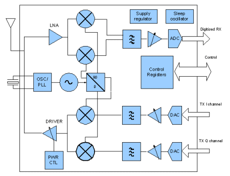
Figure 1. IEEE802.15.4 Radio System
The VCO uses a novel approach to generate the required accurate quadrature outputs over the band without resorting to use of a double speed oscillator with the associated high speed dividers. The VCO is run at two thirds of the required frequency and is then mixed with half its frequency, obtained from a simple divider. The divider provides the two quadrature outputs required. The benefit of this approach is in supplying an accurate quadrature VCO signal without the need to run functions at double the required signal, with consequent power savings. The synthesiser is a straightforward integer–N design, allowing the device to be programmed to any of the required 802.15.4 frequencies. Due to the nature of analogue IP, the radio function needs to be supplied as a hard macro, or layout, for the target process technology, in this case an 0.18um RF CMOS process. As a side issue, with a knowledge of the various possible target process design rules, the design and layout can be implemented so as to minimise the additional effort required in order to retarget the design to an alternative process.
The modem function – Figure 2, is required to translate between the 2Mc/s data emerging from the radio system and the 250kb/s data processed by the baseband system. In the transmit direction, this is relatively straightforward. The incoming groups of 4 bits are translated into the relevant 32 chip sequence using a look-up table. The sequence can then be divided into the required I & Q channels and the half sine filtering applied. This data can then be fed directly to the radio system input D/A converter. The receiver is considerably more complex. The first requirement for the modem is to set the gain of the radio system to achieve full scale deflection of the analogue to digital converter. This is performed using an algorithm which converges in the quickest possible time for all levels of input signal. With the signal at a consistent level, further processing can take place. In order to be able to demodulate the O-QPSK modulation, any frequency errors between the transmitter and receiver must first be removed. IEEE802.15.4 allows for up to +/-40ppm frequency error, so the demodulator must be able to account for up to 200kHz total frequency offset. This is performed using a frequency correction loop operating, like the AGC loop, during the preamble. With the frequency errors removed, symbol recovery can be performed and correlation techniques used to extract the original data.
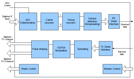
Figure 2. Modem
Implementation of the Medium Access Controller (MAC), can be split into two sets of functions which can be implemented by either hardware or software. In this particular instance, it is important that power is minimised and processor capability is retained to run applications. In order to achieve these requirements, the MAC can be split in two, with the lower layers implemented by hardware and the higher ones in software. Hardware accelerators are used to implement the automatic functions of packet formatting /deformatting, generation of the various system timers needed, automatic acknowledgement generation etc (Figure 3). This block also includes the important function of power control, particularly managing the transitions from sleep mode to operational. In the case of the 802.15.4 standard, the AES encryption functionality can also be implemented as hardware within the MAC baseband block. The use of a hardware implementation in this way optimises the availability of the system microcontroller for running the applications. The modem and baseband controller would typically be implemented as RTL descriptions, verified by synthesis to the target technology. In the case of “Chip Level IP”, they become hard macros in the same fashion as the radio system, on the target technology.
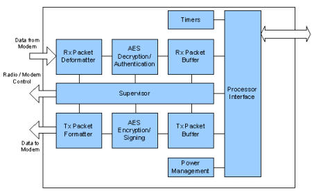
Figure 3. Baseband Controller
With a hardware implementation of much of the MAC, the software requirements are much reduced. The software tasks reduce largely to implementing packet scheduling and management tasks such as superframe / beacon management, Security management etc. The software would typically be supplied as C code, together with a complied version for the target processor.
Whilst the IP blocks form a significant portion of the development effort required for a practical implementation, there are many other design tasks that need to be performed in order to implement a single chip device. From the perspective of an IP provider, the existence of a standard targeted at a particular set of applications means that the majority of the design requirements can be specified as standard, leaving a very small subset, mainly relating to IO and memory that require customisation for individual end users of the device. Taking the example of the IEEE 802.15.4 standard, the majority of applications will require very low average power consumption, some form of analogue and digital interfaces and sufficient excess processing power to implement simple applications and networking functions. From these basic requirements, it is possible to specify a “Chip Level IP” block which forms the basis for a range of implementations that are specific to individual customer requirements. Little additional design work is then required to complete a particular implementation. Whilst moving the supply of IP to a higher level of integration, the approach does not damage the traditional model of supplying individual IP blocks to customers with particular requirements. The generation of Chip Level IP also provides the much needed practical verification of the individual IP blocks. However, it should also be noted that the Chip Level IP suffers from the same disadvantage as much analogue IP, in that it is by definition targeted at a single technology. This is resolved in the same fashion as for analogue / RF IP in that a porting exercise can be performed as a design services contract to move the design to an alternative process if required.
Taking the IEEE802.15.4 example, a range of functionality, in addition to the four main IP blocks, must be implemented in order to realise a usable single chip system; An effective power management system, including voltage regulators must be implemented in order to reduce the average power consumption as much as possible; A suitable microcontroller and memory system must be introduced; A control system which sequences the individual IP blocks to suit the standard is required; An IO subsystem is required to interface the transceiver system to the external world. Adding this functionality to the basic IP enables a single chip design to be realised which will provide a “Chip level IP” block which is close to the majority of user chip requirements – Figure 4.
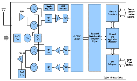
Figure 4. “Chip Level IP” for Single Chip Transceiver
Consideration of the requirements for the performance of the whole chip has significant benefits for the overall performance of the device. This is particularly true in the area of power management for very low power operation, particularly for battery operation. Treatment of this requirement for the whole chip leads to specific needs for power domains and for custom design of particular segments of the circuitry. For example, particular attention can be paid to the schematic design and power supply strategy for critical components such as the sleep timer oscillator and counter and the wake-up procedures. These can be optimised for the application. Likewise, taking a system view allows the optimum distribution of voltage regulators, again partitioned in order to optimise the wake-up procedures and hence minimise power consumption. Another example is the interaction between the radio and the modem. These can be fully analysed at a chip level, enabling issues such as AGC gain settling time or I&Q phase and amplitude imbalance to be addressed at an early stage. Finally, there are a whole range of issues relating to the integration of analogue/RF and digital blocks on the same chip. These are too complex to consider here, but a detailed treatment can be found in Ref 2. These are problems that require solving for any implementation and as such, are addressed by the adoption of a “Chip Level IP” design approach, offering the end user a higher degree of confidence in the end product.
Conclusions:
The concept of Chip Level IP provides an IP based solution for the timely and cost effective realisation of silicon systems. It is particularly effective when addressing standards based applications such as the IEEE802.15.4 example used in this paper. For standards such as these, customer specific semiconductor products can be generated (differing mainly in the provision of differing IO subsystems) providing them with products which address the application effectively with the minimum of development effort and in the quickest possible timescale.
References:
Sheffield, UK
Abstract :
The development of wireless standards designed for low cost, low power transmission of data has led to the commercial availability of single chip devices to address the smallest, lowest cost applications with a low board level design and cost overhead. Examples of this approach include the plethora of devices addressing the Bluetooth market, and a more limited range covering the proprietary low power wireless applications. Correspondingly, a range of IP blocks are available from a number of vendors, addressing the main functions required by these standards. However, these typically cover just the key blocks required, and have not fully followed the trend for single chip solutions. This paper presents an argument for the development of "Chip level IP" for single chip solutions for low power wireless systems, with particular reference to the IEEE802.15.4 standard. The standalone IP needed for such a system is described, along with the requirements for typical single chip designs. The issues involved in the integration of the basic IP to form a single chip design which forms the "Chip level IP" for this standard are discussed in detail.
"CHIP LEVEL IP" FOR LOW POWER SINGLE CHIP WIRELESS TRANSCEIVERS
The concept of the single chip wireless transciever is becoming commonplace, largely due to the success of the Bluetooth device manufacturers. From the early "Single chip" designs which required many peripheral passive and active components in order to operate correctly, a range of highly integrated devices have emerged which provide a true single chip solution for a number of high volume applications.
For this market, there are a diverse range of commercially available IP offerings, ranging from individual RF building blocks (LNA, VCO etc) through radio system designs (RF to baseband conversion) to stand-alone protocol stacks and baseband designs. However, this approach only offers a partial solution to companies wishing to facilitate the design of their own Single Chip Transceiver ICs by taking advantage of IP. A substantial amount of effort is still required to produce a competitive solution from the individual IP blocks available and this may not be commercially viable, particularly where the production volumes for a particular design are lower. An alternative approach, particularly where the requirement is to address a product defined by international standards, is to generate “Chip Level IP”. This needs to solve all of the integration problems for the chip design whilst simultaneously leaving some flexibility for customisation to allow end customers to offer differentiated products.
There are a number of emerging standards which will benefit from the availability of IP supporting them. One example is the recent IEEE802.15.4 low power wireless PHY/MAC standard which will be used by applications in the emerging ZigBee arena for low power wireless systems. This standard offers low data rate communications through a protocol which allows systems to operate with very large numbers of nodes and at very low duty cycles, allowing them to achieve very long battery life. This makes it ideal for applications such as industrial sensors and home or factory automation. A good example is the wireless light switch, where duty cycles are extremely low indeed, yet there is also a requirement for low latency and battery life of several months, or years. The 802.15.4 standard provides for latency of less than 30ms for such a device, enabling fast responses with the possibility of very low duty cycles. The availability of this standard allows standards based solutions, with the consequent benefits of interworking and security, to be adopted in place of the incumbent proprietary solutions which currently address these markets,.
IEEE802.15.4 provides for two different PHY layers, one operating in the 868MHz (in Europe) or 902-928MHz (in the USA) bands and using BPSK modulation, and one in the worldwide 2.4-2.5GHz ISM band which uses Offset QPSK modulation. The examples in this paper relate to the latter frequency band. The standard provides 16 available channels, spaced at 5MHz intervals across the band. The raw data at 250kb/s is encoded using a robust modulation scheme, transmitting one of 16 nearly orthogonal 32 chip sequences to represent 4 bits of actual data, giving, an on air chip rate of 2Mc/s. The on-air modulation scheme used is Offset QPSK, that is, QPSK with the I and Q channels offset by half a symbol. This ensures that transmitted changes result only in phase change, with minimal amplitude variations. The chipping is filtered using a half sine pulse. This scheme is extremely robust, providing a degree of protection against interferers, contributing to low power consumption by minimising any retransmission of failed packets. Further robustness is added by the use of CSMA/CA techniques to establish that the channel is clear before transmission, and the optional use of a beaconing system to allocate timeslots for transmission. Further features of the protocol are the inclusion of AES encryption, providing a high degree of security where required, and 64 bit addressing, effectively providing for an unlimited number of nodes in a given network. A more detailed treatment of the standard can be found in Ref. 1.
To support wireless standards like this, 4 major pieces of IP are required - the Radio, the baseband Modem functionality, Baseband MAC hardware and the protocol stack. These are commonly offered as individual pieces of the jigsaw. However, a key element is often missing and regularly underestimated - the remaining engineering processes required to integrate the IP, and any other functionality needed, into a commercially viable IC. Furthermore, careful consideration of the requirements for, say, power saving, can have a significant influence on the design of the system as a whole. The resolution of this conundrum is for the IP provider to take the designs one step further, and produce a "reference design" which is both a demonstration of the performance of the individual pieces of IP and a ready made design that can be readily taken into production with relatively minor modifications.
We shall discuss the individual IP blocks briefly and consider how they are integrated to produce a single chip solution. As IP blocks, the generic requirements are that the designs are robust, will be tolerant of process porting and provide excellent performance with low power consumption.
The Radio System – Figure 1, is required to translate between the 2.4GHz on air signals and the baseband signals that can be handled by the subsequent signal processing. To minimise the power consumption by reducing the number of filters and data converters, the system uses a low IF architecture in receive, and a quadrature modulater operating on the VCO in transmit. Particular attention must be paid to reduction of the necessary external circuitry, e.g. all the required matching in order to interface to a resistive balanced antenna should be included on the chip. In the receive chain, the channel filter provides attenuation in excess of the requirements specified in the standard. This is in order to increase the robustness of the system in a noisy environment – a key feature in the drive to minimise packet retransmissions. Variable gain amplifiers are provided to allow a full signal swing to be presented to the ADC regardless of the input RF signal level. A single analogue to digital converter digitises the signal for transfer to the modem. In the transmit direction, a conventional quadrature modulator adds the O-QPSK modulation to the VCO.

Figure 1. IEEE802.15.4 Radio System
The VCO uses a novel approach to generate the required accurate quadrature outputs over the band without resorting to use of a double speed oscillator with the associated high speed dividers. The VCO is run at two thirds of the required frequency and is then mixed with half its frequency, obtained from a simple divider. The divider provides the two quadrature outputs required. The benefit of this approach is in supplying an accurate quadrature VCO signal without the need to run functions at double the required signal, with consequent power savings. The synthesiser is a straightforward integer–N design, allowing the device to be programmed to any of the required 802.15.4 frequencies. Due to the nature of analogue IP, the radio function needs to be supplied as a hard macro, or layout, for the target process technology, in this case an 0.18um RF CMOS process. As a side issue, with a knowledge of the various possible target process design rules, the design and layout can be implemented so as to minimise the additional effort required in order to retarget the design to an alternative process.
The modem function – Figure 2, is required to translate between the 2Mc/s data emerging from the radio system and the 250kb/s data processed by the baseband system. In the transmit direction, this is relatively straightforward. The incoming groups of 4 bits are translated into the relevant 32 chip sequence using a look-up table. The sequence can then be divided into the required I & Q channels and the half sine filtering applied. This data can then be fed directly to the radio system input D/A converter. The receiver is considerably more complex. The first requirement for the modem is to set the gain of the radio system to achieve full scale deflection of the analogue to digital converter. This is performed using an algorithm which converges in the quickest possible time for all levels of input signal. With the signal at a consistent level, further processing can take place. In order to be able to demodulate the O-QPSK modulation, any frequency errors between the transmitter and receiver must first be removed. IEEE802.15.4 allows for up to +/-40ppm frequency error, so the demodulator must be able to account for up to 200kHz total frequency offset. This is performed using a frequency correction loop operating, like the AGC loop, during the preamble. With the frequency errors removed, symbol recovery can be performed and correlation techniques used to extract the original data.

Figure 2. Modem
Implementation of the Medium Access Controller (MAC), can be split into two sets of functions which can be implemented by either hardware or software. In this particular instance, it is important that power is minimised and processor capability is retained to run applications. In order to achieve these requirements, the MAC can be split in two, with the lower layers implemented by hardware and the higher ones in software. Hardware accelerators are used to implement the automatic functions of packet formatting /deformatting, generation of the various system timers needed, automatic acknowledgement generation etc (Figure 3). This block also includes the important function of power control, particularly managing the transitions from sleep mode to operational. In the case of the 802.15.4 standard, the AES encryption functionality can also be implemented as hardware within the MAC baseband block. The use of a hardware implementation in this way optimises the availability of the system microcontroller for running the applications. The modem and baseband controller would typically be implemented as RTL descriptions, verified by synthesis to the target technology. In the case of “Chip Level IP”, they become hard macros in the same fashion as the radio system, on the target technology.

Figure 3. Baseband Controller
With a hardware implementation of much of the MAC, the software requirements are much reduced. The software tasks reduce largely to implementing packet scheduling and management tasks such as superframe / beacon management, Security management etc. The software would typically be supplied as C code, together with a complied version for the target processor.
Whilst the IP blocks form a significant portion of the development effort required for a practical implementation, there are many other design tasks that need to be performed in order to implement a single chip device. From the perspective of an IP provider, the existence of a standard targeted at a particular set of applications means that the majority of the design requirements can be specified as standard, leaving a very small subset, mainly relating to IO and memory that require customisation for individual end users of the device. Taking the example of the IEEE 802.15.4 standard, the majority of applications will require very low average power consumption, some form of analogue and digital interfaces and sufficient excess processing power to implement simple applications and networking functions. From these basic requirements, it is possible to specify a “Chip Level IP” block which forms the basis for a range of implementations that are specific to individual customer requirements. Little additional design work is then required to complete a particular implementation. Whilst moving the supply of IP to a higher level of integration, the approach does not damage the traditional model of supplying individual IP blocks to customers with particular requirements. The generation of Chip Level IP also provides the much needed practical verification of the individual IP blocks. However, it should also be noted that the Chip Level IP suffers from the same disadvantage as much analogue IP, in that it is by definition targeted at a single technology. This is resolved in the same fashion as for analogue / RF IP in that a porting exercise can be performed as a design services contract to move the design to an alternative process if required.
Taking the IEEE802.15.4 example, a range of functionality, in addition to the four main IP blocks, must be implemented in order to realise a usable single chip system; An effective power management system, including voltage regulators must be implemented in order to reduce the average power consumption as much as possible; A suitable microcontroller and memory system must be introduced; A control system which sequences the individual IP blocks to suit the standard is required; An IO subsystem is required to interface the transceiver system to the external world. Adding this functionality to the basic IP enables a single chip design to be realised which will provide a “Chip level IP” block which is close to the majority of user chip requirements – Figure 4.

Figure 4. “Chip Level IP” for Single Chip Transceiver
Consideration of the requirements for the performance of the whole chip has significant benefits for the overall performance of the device. This is particularly true in the area of power management for very low power operation, particularly for battery operation. Treatment of this requirement for the whole chip leads to specific needs for power domains and for custom design of particular segments of the circuitry. For example, particular attention can be paid to the schematic design and power supply strategy for critical components such as the sleep timer oscillator and counter and the wake-up procedures. These can be optimised for the application. Likewise, taking a system view allows the optimum distribution of voltage regulators, again partitioned in order to optimise the wake-up procedures and hence minimise power consumption. Another example is the interaction between the radio and the modem. These can be fully analysed at a chip level, enabling issues such as AGC gain settling time or I&Q phase and amplitude imbalance to be addressed at an early stage. Finally, there are a whole range of issues relating to the integration of analogue/RF and digital blocks on the same chip. These are too complex to consider here, but a detailed treatment can be found in Ref 2. These are problems that require solving for any implementation and as such, are addressed by the adoption of a “Chip Level IP” design approach, offering the end user a higher degree of confidence in the end product.
Conclusions:
The concept of Chip Level IP provides an IP based solution for the timely and cost effective realisation of silicon systems. It is particularly effective when addressing standards based applications such as the IEEE802.15.4 example used in this paper. For standards such as these, customer specific semiconductor products can be generated (differing mainly in the provision of differing IO subsystems) providing them with products which address the application effectively with the minimum of development effort and in the quickest possible timescale.
References:
- Ref. 1: Home Networking with IEEE802.15.4: A Developing Standard for Low Rate Wireless Personal Area Networks; IEEE Communications Magazine, August 2002, vol 40, no 8; Ed Callaway et al.
- Ref 2. “Simulation Techniques and Solutions for Mixed-Signal Coupling in Integrated Circuits” by N.K. Verghese, T.J.Schmerbeck and D.J.Allstot. Published by Kluwer Academic publishers.
Related Semiconductor IP
- Ultra-Low-Power LPDDR3/LPDDR2/DDR3L Combo Subsystem
- 1G BASE-T Ethernet Verification IP
- Network-on-Chip (NoC)
- Microsecond Channel (MSC/MSC-Plus) Controller
- 12-bit, 400 MSPS SAR ADC - TSMC 12nm FFC
Related Articles
- The pivotal role power management IP plays in chip design
- A Design of System on a Chip for Voice over Wireless LAN
- System on Chip (SoC) for Short Range Wireless - CMOS versus SIGe
- A Chip IP Integrator for System Level Design
Latest Articles
- Extending and Accelerating Inner Product Masking with Fault Detection via Instruction Set Extension
- ioPUF+: A PUF Based on I/O Pull-Up/Down Resistors for Secret Key Generation in IoT Nodes
- In-Situ Encryption of Single-Transistor Nonvolatile Memories without Density Loss
- David vs. Goliath: Can Small Models Win Big with Agentic AI in Hardware Design?
- RoMe: Row Granularity Access Memory System for Large Language Models