DO-254 IP
Filter
Compare
94
IP
from
13
vendors
(1
-
10)
-
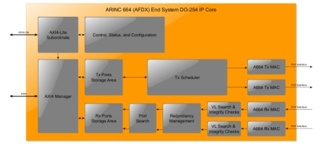
ARINC 664 (AFDX) End System DO-254 IP Core
- The ARINC 664 (AFDX) End System DO-254 IP Core (AFDX ES IP) implements an AFDX End System as specified in ARINC 664 Part 7 “Avionics Full-Duplex Switched Ethernet (AFDX) Network”.
- The AFDX ES IP supports MII, RMII, GMII or SGMII as PHY interfaces. Therefore, it is able to transmit and receive at 10 Mbps, 100 Mbps or 1000 Mbps, making full usage of the bandwidth.
-
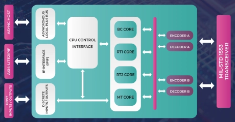
DO-254 compliant MIL-STD-1553B IP core
- MIL-STD-1553B IP Core implements MIL-STD-1553B standard and provides single or multi-functional interface between host processor and MIL-STD-1553 bus transceiver.
- DO-254 compliant MIL-STD-1553B IP core can function as Bus Controller (BC), two separate Remote Terminals (RT) and Bus Monitor (BM), simultaneously.
-
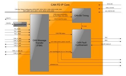
CAN FD Controller DO-254 IP Core
- The CAN FD Controller implements a Controller Area Network as specified in the ISO 11898:2015 Part 1, supporting both Classical and Flexible Data Rate CAN frame formats.
- The CAN FD Controller supports bit rates up to 1 Mbit/s for Classical CAN frame format and up to 10Mbit/s for Flexible Data Rate format.
-
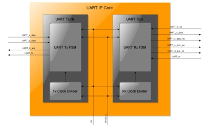
UART DO-254 IP Core
- The Universal Asynchronous Receiver/Transmitter (UART) is a hardware device that translates data between parallel and serial forms.
- UARTs are commonly used in conjunction with communication standards such as TIA (formerly EIA) RS-232, RS-422 or RS-485.
-
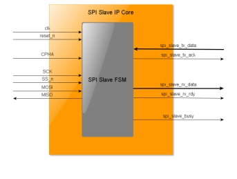
SPI Slave DO-254 IP Core
- The SPI Slave IP Core implements an SPI Slave fully compliant to the SPI Standard (Motorola’s M68H11 Reference Manual).
- The Serial Peripheral Interface (SPI) bus is a synchronous serial communication interface specification used for short distance communication, primarily in embedded systems.
-
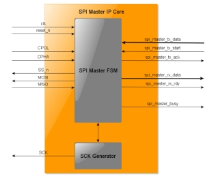
SPI Master DO-254 IP Core
- The SPI Master IP Core implements an SPI Master fully compliant to the SPI Standard (Motorola’s M68H11 Reference Manual).
- The Serial Peripheral Interface (SPI) bus is a synchronous serial communication interface specification used for short distance communication, primarily in embedded systems.
-
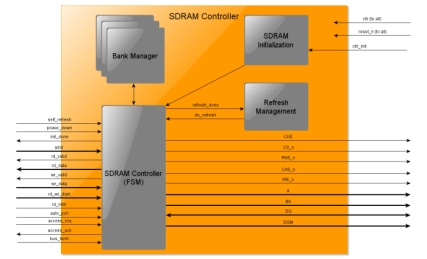
SDRAM Controller DO-254 IP Core
- The SDRAM Controller implements a controller for Single Data Rate Synchronous Dynamic Random Access Memory (SDR SDRAM) devices as specified in the JEDEC Standard No. 21-C Page 3.11.5.1 Release 12.
- Single Data Rate SDRAM can accept one command and transfer one word of data per clock cycle.
-
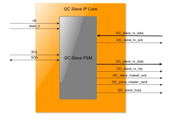
I2C Slave DO-254 IP Core
- The I2C Slave IP Core implements an I2C Slave fully compliant to the I2C-bus specification and user manual Rev. 5 – 9 October 2012 for Standard-mode, Fast-mode and Fast-mode Plus (Fm+).
- The Inter-Integrated Circuit (I2C) is a multi-master, multi-slave, single-ended, serial computer bus invented by Philips Semiconductor (now NXP Semiconductors).
-
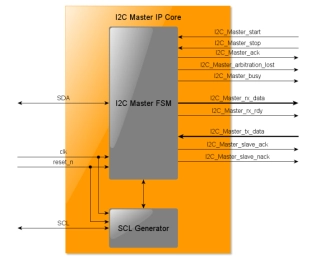
I2C Master DO-254 IP Core
- Design Assurance Level A according to RTCA DO-254/ED-80 (April, 2000)
- Fully compliant to the I2C-bus specification and user manual Rev. 5 – 9 October 2012 for Standard-mode, Fast-mode and Fast-mode Plus (Fm+)
- Configurable data rate (100kHz, 400kHz or 1000kHz)
- Support for all Options (Multi-master, Synchronization, Arbitration, Clock stretching, 10-bit slave address, General Call address, Software Reset and START byte)
-
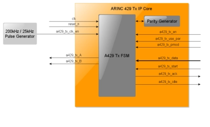
ARINC 429 Transmitter DO-254 IP Core
- The ARINC 429 Tx IP Core implements a transmitter as specified in the ARINC Specification 429 Part 1-17.
- The ARINC 429 Rx Core has been developed to DAL A according to the DO-254 / ED-80 and is accompanied by a Certification Kit.
