CES 2026 Recap: Trust Built on a Real, Working eUSB2V2 System Demo
Nothing builds trust like a real working system.
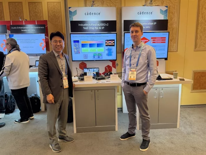
That was the guiding principle behind our CES 2026 showcase in Las Vegas—where we successfully demonstrated what we believe is an industry-first 3nm eUSB2V2 PHY IP alongside eUSB2V2 controller IPs (both host and device) running together in a complete, end-to-end system. The result: a live, real-world eUSB2V2 data path performing at speeds of up to 4.8 Gbps, highlighting the promise of this new USB interface protocol.
Why This Demo Mattered
When a new interface technology emerges, specs and simulations are only part of the story. What customers and partners truly need is confidence that the ecosystem can work, in practice, across chips, controllers, PHYs, platforms, and devices.
At CES 2026, we brought that confidence to life with a demo designed to answer a simple question: Can eUSB2V2 deliver real throughput in real conditions—with real system behavior and interoperability?
Our answer: Yes, live, on the show floor.
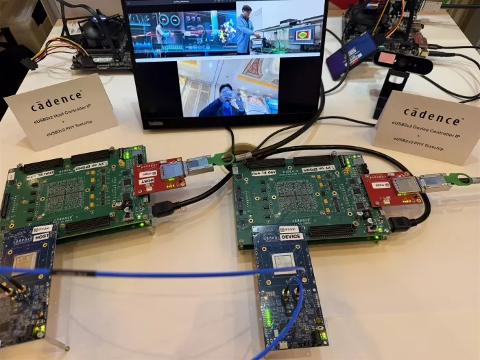
Demo Setup: A Complete Device to Host the eUSB2V2 System
The demo system was built to represent a realistic, end-to-end data flow—capturing video on the device side and delivering it reliably to the host side for processing and display.
System architecture (high level):
- 3nm eUSB2V2 PHY test chips on both host and device sides
- Host and device controllers implemented on FPGA boards
- PC/ATX boards in the loop to support the full end-to-end pipeline
- SMA cable connectivity between device PHY and host PHY to ensure robust signal integrity
- Monitor display on the host side showing the live video feed
Explore eUSB2V2 IP:
How Data Flowed
A high-resolution camera streamed maximum raw data in real time through the PC/ATX boards into the FPGA-based system. The device PHY communicated to the host PHY over SMA, and on the host side, the FPGA board ran the host controller, connecting to a PC/ATX board and monitor to display the live captured video.
This seamless flow showcased the efficiency and performance of eUSB2V2 in a practical, real-world scenario—not just a lab bench proof.
The Highlight: Two Simultaneous 4K Video Streams Over eUSB2V2
To push the system beyond a single “happy path” workload, we demonstrated two video sources transferring simultaneously from the eUSB2V2 device side to the eUSB2V2 host side.
1. 4K Live Video (UVC) — Uncompressed YUV
One stream was a 4K live video feed captured from a 4K webcam, transported as uncompressed YUV video from the device side to the host side. On the host, the system SoC performed video enhancement and rendered the output to the monitor.
- Protocol/class used: UVC (USB Video Class)
- Key takeaway: eUSB2V2 can sustain demanding real-time video movement without relying on compression tricks.
2. 4K Recorded Video (MSC) — Bulk Transfer from SSD
The second stream demonstrated bulk data transfer: a 4K recorded video stored on an SSD acting as the device. The host system received the content and rendered it on the display.
- Protocol/class used: MSC (Mass Storage Class)
- Key takeaway: eUSB2V2 supports high-throughput bulk workloads alongside real-time streaming.
A Critical Enabler: UTMI v2.0 Bridging Controller and PHY
A key element of the demo was how we connected the system pieces cleanly and correctly.
- Controllers (host + device): running on Cadence FPGA platforms
- 3nm PHY IP: implemented in test chips
- Bridge/interface: the newly published UTMI (USB 2.0 Transceiver Macrocell Interface) v2.0
This enabled a smooth connection between the controller IP in FPGA and the PHY IP in silicon—helping validate the full stack of the solution.
What This Proves: eUSB2V2 As a Complete Solution
This CES 2026 demonstration wasn’t just a speed milestone. It was a system-level proof that eUSB2V2 can be delivered as a complete, interoperable solution:
- Industry-first 3nm eUSB2V2 PHY IP (host + device PHY coverage)
- Host and device controller IPs
- A validated, real-time system that shows how the pieces operate together in the field
And importantly, it provides confidence for adoption—especially because it supports seamless interoperability between:
- Host-side solutions already licensed by tier-1 customers, and
- A variety of device-side solution providers across the ecosystem
Looking Forward: Built for What's Next – Consumer and Edge AI
Beyond consumer connectivity, this milestone reflects a strategic direction toward the anticipated edge AI era—where bandwidth, latency, power efficiency, and reliability become increasingly critical for distributed intelligence and sensor-rich devices.
This is about showing not only what’s possible today—but what can scale into next-generation applications tomorrow.
Conclusion
eUSB2V2 delivers the flexibility modern systems demand, combining high data rates, configurable link options, reduced EMI, and low power operation. As SoCs move to advanced process nodes while connected devices remain on mature nodes, eUSB2V2 is quickly becoming the go-to USB interface to bridge the gap, extending the proven, ubiquitous USB ecosystem.
Cadence, a long-time leader in USB IP, has expanded its portfolio with complete, end-to-end eUSB2V2 solutions, including host and peripheral controllers, PHYs, drivers, and Verification IP. Learn more at cadence.com
Related Semiconductor IP
Related Blogs
- Industry’s First End-to-End eUSB2V2 Demo for Edge AI and AI PCs at CES
- Cadence Transforms Chiplet Technology with First Arm-Based System Chiplet
- Cadence Announces Industry's First Verification IP for Embedded USB2v2 (eUSB2v2)
- AMBA LTI Verification IP for Arm System MMU
Latest Blogs
- Area, Pipelining, Integration: A Comparison of SHA-2 and SHA-3 for embedded Systems.
- Why Your Next Smartphone Needs Micro-Cooling
- Teaching AI Agents to Speak Hardware
- SOCAMM: Modernizing Data Center Memory with LPDDR6/5X
- Bridging the Gap: Why eFPGA Integration is a Managed Reality, Not a Schedule Risk