The On-Device LLM Revolution: Why 3B-30B Models Are Moving to the Edge

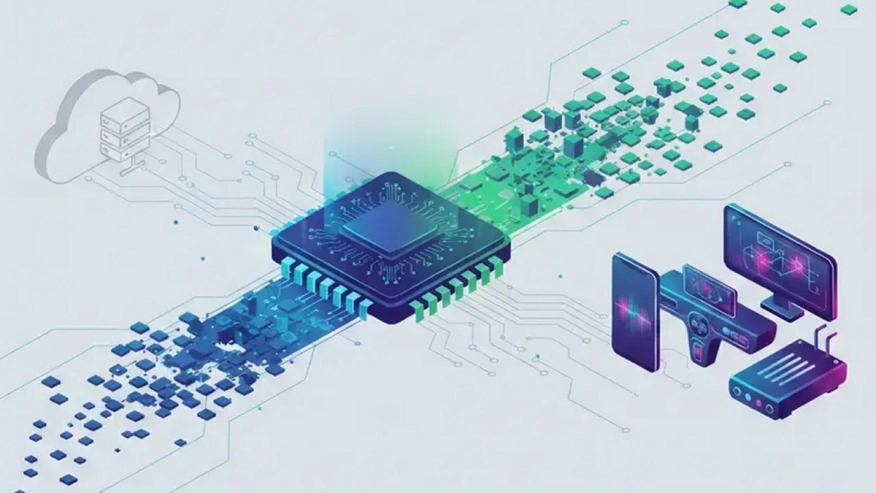
After years of cloud-centric inference, AI is moving to the edge. The "Goldilocks zone" of 3B to 30B parameter models is delivering GPT-4-class performance on smartphones, automotive systems, and industrial equipment — and creating an acute challenge for silicon designers.
 The AI world is experiencing a fundamental shift. After years of cloud-centric inference dominated by massive data center GPUs, we're witnessing an accelerating migration of language models to edge devices. Not the trillion-parameter behemoths that require server farms, but the "Goldilocks zone" models: 3B to 30B parameters — large enough to deliver genuinely useful AI capabilities, small enough to run locally on everything from smartphones to automotive systems to industrial equipment.
This isn't a passing trend. It's an architectural inflection point driven by latency requirements, privacy mandates, cost pressures, and user experience demands that cloud inference simply cannot satisfy. And it's creating an acute problem for silicon designers: how do you build processing solutions that can actually deliver on this promise?
The Sweet Spot: 3B to 30B Parameters
Consider what's happening in the model landscape. Llama 3.2 3B. Phi-3 3.8B. Gemma 7B. Mistral 7B. Qwen3-30B-A3B using Mixture-of-Experts to activate just 3.3B parameters per token while maintaining 30B total parameter capability. These aren't toy models — they're delivering GPT-4-class performance on specific tasks while fitting in the thermal and power envelopes of edge devices.
Users running a quantized 7B model on a laptop expect 40+ tokens per second. A 30B MoE model on a high-end mobile device should hit 30+ tokens/second. Anything less feels broken. Cloud latency of 500ms+ round-trip? Completely unacceptable for real-time applications. The bar has been set, and it's high.
But here's the catch: delivering those performance levels sustainably, in production silicon, at edge power budgets, while remaining adaptable to the next model architecture that drops next month? That's where most AI accelerator solutions fall apart.
The Processing Challenge No One's Solving
Running LLMs at the edge requires threading several needles simultaneously:
Tokens per second performance that users actually notice. It's not just about hitting some theoretical TOPS number on a datasheet. It's about sustainable throughput on real models with real context lengths. A solution that delivers 50 tokens/second on a 7B model in ideal conditions but drops to 8 tokens/second with a 16K context window isn't a solution — it's a science project.
Power efficiency that fits the platform. Data center accelerators consume hundreds of watts. Edge devices measure their power budgets in single-digit watts. A smartphone SoC can't accommodate a 50W AI accelerator. An automotive system needs ASIL-ready safety certification. Industrial equipment needs to operate in temperature extremes. The processing solution has to deliver AI performance within these constraints, not despite them.
Programmability for model evolution. Here's what everyone building fixed-function NPUs discovered the hard way: AI model architectures evolve faster than silicon development cycles. The accelerator you taped out for ResNet doesn't run transformers well. The one optimized for transformers struggles with Mixture-of-Experts. The one built for today's attention mechanisms won't efficiently handle whatever novel architecture researchers publish next quarter.
True programmability — not "configurable within preset options" but genuine C++ programmability that lets you map new operators, new quantization schemes, new attention mechanisms without waiting for your IP vendor to maybe support it in their next release — is the only way to future-proof silicon investments.
SoC integration without dominating the chip. Most edge platforms aren't AI-first devices. They're smartphones, cars, printers, robots, industrial controllers where AI is one function among many. AI acceleration needs to integrate as a component in a heterogeneous SoC, not demand that the entire chip be designed around it.
Why GPUs Don't Fix This
The knee-jerk response: "Just use a GPU." But GPUs optimized for data center training bring fundamental mismatches to edge inference:
Power consumption incompatible with battery operation or thermally constrained enclosures. Die area and cost structures designed for discrete cards, not integrated SoCs. Memory bandwidth requirements that strain mobile memory subsystems. And critically, architectures that batch-process inference for maximum throughput — exactly wrong for the latency-sensitive, single-batch inference that edge applications demand.
A GPU might hit impressive TOPS numbers, but if it consumes 75W to generate 30 tokens/second when the application needs 3W to generate the same 30 tokens/second, it's the wrong tool for the job.
The Legacy NPU Trap
Five or six years ago, CPU and DSP IP vendors rushed into neural processing by bolting matrix accelerators onto their existing products. The logic seemed sound: "Use our trusted CPU/DSP and offload those compute-hungry matrix operations to an accelerator." Quick time to market. Minimal disruption to existing product lines.
The fatal flaw: algorithm partitioning. These architectures force developers to split AI workloads across multiple compute engines — some layers on the NPU accelerator, some on the CPU, some on the DSP. As long as the "cuts" in the algorithm remained minimal (ResNet: one partition at the end), these solutions worked. But transformers arrived with vastly different operator distributions. Suddenly the "accelerator" couldn't accelerate most of the model. Performance collapsed. Customers ate expensive respins.
The vendors responded predictably: "Here's our second-generation accelerator!" Which worked... until the next model architecture shift. Now we're seeing third-generation attempts, each time promising "this one handles everything forever." But the fundamental architectural trap remains: fixed-function acceleration of a moving target.
What Actually Works
The edge AI processing challenge demands a different architectural philosophy. Not "CPU plus accelerator" or "fixed-function NPU." A processor that's genuinely programmable yet delivers acceleration-class efficiency. A single unified architecture that runs the complete AI graph — preprocessing, inference, postprocessing — without partitioning across multiple engines.
Quadric's Chimera GPNPU delivers exactly this. It's not a matrix accelerator bolted onto something else. It's a purpose-built general-purpose neural processing unit where every compute tile integrates both matrix acceleration (MACs) and full 32-bit programmable ALUs in fine-grained, tightly coupled architecture.
That 1024-tile Chimera QC Ultra core? That's 1024 MAC units for matrix operations. And 1024 fully programmable 32-bit ALUs. Operating in unison on the same instruction. That's 32,768 bits of parallel, C++-programmable compute. All accessible through a single instruction fetch, a single AXI port, with data locality maintained within the tile.
The result: matrix acceleration performance when you need it, full programmability when model architectures demand it, all in a unified architecture that doesn't force algorithm partitioning.
Explore NPU IP:
- GPNPU Processor IP - 32 to 864TOPs
- Safety Enhanced GPNPU Processor IP
- GPNPU Processor IP - 4 to 28 TOPs
- GPNPU Processor IP - 1 to 7 TOPs
Performance That Matters
Tokens per second on real models, at real power levels, with real quantization schemes:
A Chimera core running a quantized 7B parameter model delivers competitive throughput — the kind users expect from cloud services — at power levels appropriate for edge deployment. Need more performance? Chimera scales across multiple cores in the same SoC fabric without architectural compromises.
The architecture handles INT8, INT4, mixed precision, even custom quantization schemes. Not because we predicted every possible format, but because the underlying compute is genuinely programmable. When a new quantization technique appears, it's a software update, not a hardware redesign request to your IP vendor followed by a 12-month wait.
Models from 3B to 30B parameters all map efficiently. Transformers, MoE architectures, whatever researchers publish next — they all run on the same Chimera core because the architecture provides the fundamental compute primitives rather than hard-coding specific operator implementations.
The SoC Integration Reality
Chimera integrates into heterogeneous SoCs alongside CPUs, traditional GPUs, DSPs, and other specialized blocks. It shares memory bandwidth efficiently. It operates within realistic power budgets — single-digit watts for meaningful AI performance. It scales from 1 TOPS for cost-sensitive applications to 864 TOPS for advanced ADAS systems.
Because it's designed from first principles as an SoC component rather than a retrofit of data center technology, it actually fits in the products customers are building: smartphones, automotive platforms, industrial equipment, edge servers.
Why This Matters Now
On-device LLM inference isn't coming — it's here. Smartphone users expect local AI assistants that respond instantly while preserving privacy. Automotive systems need real-time natural language understanding and reasoning without cloud connectivity. Industrial robotics demand intelligent decision-making with deterministic latency. Medical devices require AI processing that keeps sensitive data local.
The applications exist. The models exist. What hasn't existed until now is processing silicon that can actually deliver: the performance users demand, at power levels products can accommodate, with the programmability to adapt as models evolve, at costs that make sense for high-volume production.
That's not a GPU problem. It's not a CPU-plus-accelerator problem. It's a new processing challenge that requires purpose-built solutions.
The Architecture Matters More Than The TOPS Number
The semiconductor industry loves simple metrics. TOPS. TOPS/watt. TOPS/mm². But for LLM inference at the edge, those numbers are almost meaningless without context.
What's the sustainable tokens/second performance on real models at real batch sizes? What happens to that performance with 16K context? With INT4 quantization? With the model architecture that hasn't been invented yet?
Can you integrate it in an SoC without dominating the power budget? Can developers actually program it without a six-month learning curve and a dedicated team from the IP vendor? Does it still work when the next LLM architecture appears?
Those are the questions that separate science projects from production silicon. And they're the questions Chimera was architected to answer.
The shift to on-device LLMs is accelerating. The models are ready. The applications are here. The silicon needs to catch up.
Learn more about Quadric's Chimera GPNPU and our approach to on-device LLM inference at quadric.ai/large-language-models.
Related Semiconductor IP
- GPNPU Processor IP - 32 to 864TOPs
- Safety Enhanced GPNPU Processor IP
- GPNPU Processor IP - 4 to 28 TOPs
- GPNPU Processor IP - 1 to 7 TOPs
- NPU
Related Blogs
- Five Architectural Reasons Why FPGAs Are the Ultimate AI Inference Engines
- Rethinking Edge AI Interconnects: Why Multi-Protocol Is the New Standard
- Why Low-Level Libraries are the Key to AI Success
- Synopsys Expands Collaboration with Arm to Accelerate the Automotive Industry’s Transformation to Software-Defined Vehicles