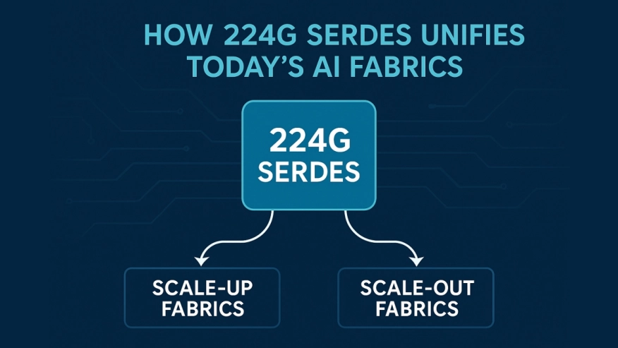
How 224G SerDes Unifies Today’s AI Fabrics
AI system architects no longer face a binary choice between scale-up and scale-out fabrics. Modern AI platforms require both to be executed efficiently, predictably, and within aggressive schedules. The shift lies in how risk is managed across these domains.
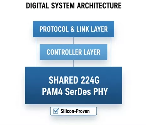
 At the physical layer, the emergence of a silicon-proven 224G PAM4 SerDes has become a unifying foundation for both scale-up and scale-out transports. By leveraging the same high-speed SerDes for UALink-based fabrics and Ethernet-based scale-out networks, teams can reuse validated silicon, streamline validation cycles, and accelerate time to tapeout. This convergence is already shaping leading AI and hyperscale designs, with the 224G SerDes serving as a common PHY foundation across diverse interconnect fabrics and protocols
One SerDes, Two Fabric Domains
AI systems span two distinct interconnect domains:
- Scale-Up Fabrics: Optimized for low latency and high bandwidth between accelerators within a node or tray.
- Scale-Out Fabrics: Designed for reach, topology flexibility, and system-level scaling across racks and rows.
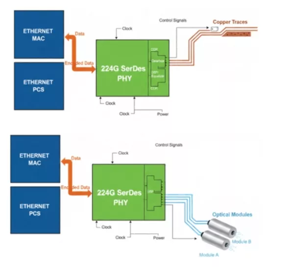
Historically, these domains required separate PHYs, channel models, and signal integrity (SI) validation. However, at 224G, this separation is dissolving. A single 224G PAM4 SerDes PHY now supports both domains, enabling short-reach links for scale-up while also providing long-reach electrical and optical interfaces for scale-out Ethernet transports.
Scale-Up: Bandwidth Density Without New PHY Risk
Scale-up fabrics, such as UALink class architectures, demand extreme bandwidth density with deterministic latency. While protocols and controllers evolve, the electrical challenges at 224G, including jitter tolerance, equalization, adaptation, and power efficiency, are well understood at the PHY layer.
By building scale-up links on a silicon-proven 224G SerDes, architects eliminate the risk of introducing untested PHY designs at the most sensitive layer. The PHY's behavior, DSP architecture, and adaptation mechanisms are inherited from production-quality designs. This allows teams to focus validation efforts on areas of differentiation, such as topology, coherence, and software stacks, rather than rediscovering physical layer fundamentals.
Scale-Out: Ethernet Evolves, PHY Risk Does Not
On the scale-out side, Ethernet continues to evolve to meet AI bandwidth demands, with 800G and 1.6T systems pushing both electrical and optical boundaries. Despite these advancements, the value of reusing a validated 224G SerDes PHY remains constant.
A production-quality 224G SerDes supports the reach, signal integrity, and power efficiency required for both copper and optical interfaces in scale-out networks and in scale-up networks. Reusing the same PHY across platforms ensures consistent channel models, reusable SI and power integrity (PI) methodologies, and reduced bring-up and compliance risk. This reuse shortens development schedules and simplifies multi-generation Ethernet roadmaps by maintaining a stable physical layer even as higher-level standards evolve.
Why Silicon-Proven Matters at 224G
At 224G, simulation alone is insufficient. The margin for error is razor-thin, and real-world effects significantly shape PHY behavior. A silicon-proven SerDes brings:
- Validated DSP and adaptation behavior for electrical and optical links
- Well-characterized power/performance tradeoffs
- Confidence across process nodes and channel types
This maturity allows teams to treat the PHY as an enabler rather than a risk factor. Consequently, innovation above the physical layer can proceed with greater confidence and predictability across both scale-up and scale-out designs.
Explore 224G SerDes IP:
A Unifying Foundation for AI Systems
The most significant shift underway is architectural rather than protocol-driven. When a single 224G SerDes PHY supports multiple AI fabrics, organizations gain:
- Design reuse across programs
- Reduced cumulative validation costs
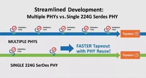
- Shortened tapeout cycles with greater schedule predictability
As AI systems scale in size and complexity, this unification at the physical layer becomes a strategic advantage. It enables teams to innovate faster without multiplying risk, maintaining a consistent electrical foundation across diverse interconnect fabrics.
Cadence Enables the Next Generation of AI Fabrics
Cadence offers a comprehensive portfolio of silicon-proven interface and memory IP, spanning 224G PAM4 SerDes, Ethernet and Ultra Ethernet PCS, and dedicated AI interconnects like UALink™. These IP solutions are architected for maximum reuse, enabling customers to deploy a unified, validated physical layer across both scale-up and scale-out fabrics. This approach not only lowers design risk but also significantly accelerates time to tapeout.
By combining high-speed SerDes and controller IP with subsystem integration, advanced-node readiness, and packaging-aware design flows, Cadence is delivering at the scale modern AI factories demand.
Learn more about Cadence IP for optical interconnect.
Related Semiconductor IP
- 224G SerDes PHY and controller for UALink for AI systems
- 224G Ethernet PHY, TSMC N3P x1, North/South (vertical) poly orientation
- 224G Ethernet PHY, TSMC N2P x4, North/South (vertical) poly orientation
- 224G Ethernet PHY, Intel 18A x4, North/South (vertical) poly orientation
- 224G Ethernet PHY in TSMC (N3E)
Related Blogs
- Cadence Perspective: 224G SerDes Trend and Solution
- How PCIe® Technology is Connecting Disaggregated Systems for Generative AI
- How SiFive is Driving AI and Datacenter Innovation
- How Physical AI Is Redefining the Automotive Industry
Latest Blogs
- A Bench-to-In-Field Telemetry Platform for Datacenter Power Management
- IDS-Verify™: From Specification to Sign-Off – Automated CSR, Hardware Software Interface and CPU-Peripheral Interface Verification
- RISC-V and GPU Synergy in Practice: A Path Towards High-Performance SoCs from SpacemiT K3
- EDA AI Agents: Intelligent Automation in Semiconductor & PCB Design
- Why Security Can't Exist Without Trust