Industry’s First End-to-End eUSB2V2 Demo for Edge AI and AI PCs at CES
Since their debut in 2023, AI PCs have taken the market by storm. Gartner projects that 77 million AI PCs will ship in 2025, representing 31% of the worldwide PC market, and growing to a 55% market share in 2026. Meanwhile, edge AI is multiplying due to a variety of factors, including smaller and more efficient AI algorithms, more powerful AI silicon, and the proliferation of IoT devices.
As laptops, AI PCs, and the latest imaging systems demand even higher performance and lower power, SoCs are challenged to keep pace. Advanced-node SoCs at 5nm and below must balance efficiency with ultra-low voltages and growing bandwidth needs. High-resolution cameras, faster frame rates, and AI-driven workloads all require interfaces that deliver speed with minimal EMI/RFI noise.
Cadence's industry-first eUSB2V2 IP addresses these very challenges, providing a robust solution for edge AI and AI PCs. Built on the advanced 3nm process and compliant with the latest eUSB2V2 standard, the Cadence eUSB2V2 solution supports up to 4.8Gbps at low I/O voltage—delivering the low power, flexible asymmetric data rates, and superior signal integrity required by modern SoCs.
Explore eUSB2V2 IP
From PHY Test Chip to Complete End-to-End Solution
Earlier this year, Cadence achieved a major milestone with the tapeout of the first 3nm eUSB2V2 PHY test chip, now fully validated and completing silicon characterization. Building on this success, Cadence has developed a complete end-to-end eUSB2V2 solution, including both host and device controller IP. At CES 2026, Cadence will showcase its industry-first, real-time end-to-end eUSB2V2 demo, integrating host and device PHYs and controllers, demonstrating real-world system performance, and paving the way for next-generation connectivity in AI PCs and edge AI systems.
Designed for flexibility, the Cadence eUSB2V2 host and device controllers are available as standalone IP replacing legacy USB 2.0 or eUSB2V1 for optimal PPA and simplicity. They can be used in combination with USB 3.2 and USB 2.0, enabling easier integration with minimal risk for complete USB subsystems. Also compliant with UTMI 2.0, the controllers support up to 4.8Gbit/s symmetric and asymmetric serial data transmission rates and high-speed (HS) native mode.
eUSB2V2 Controllers: A Deeper Dive
To help customers more easily implement eUSB2V2 in their advanced SoCs for consumer and PC devices, Cadence eUSB2V2 controllers offer several advantages, including:
- Multiple burst transaction support for isochronous endpoints within a single micro-frame maximizes utilization of available periodic bandwidth
- Increased MaxPacketSize for bulk endpoints, now supporting up to 1024 bytes, enables large data transfers to accommodate increased image sizes
- Advanced clock gating for low power consumption
- Existing USB2/USB3 ports are preserved, maintaining compliance and interoperability
- Configurable number of eUSB2V2 ports offers design flexibility
Figure 1 illustrates the eUSB2V2 controller architecture, combined with USB 3.x and USB 2.0 (eUSB2v1).
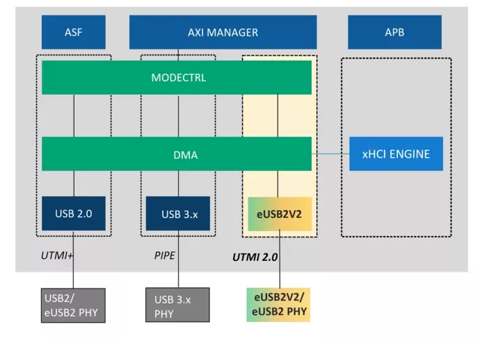
Figure 1. eUSB2V2 controller architecture
Whether you have existing multiple USB ports and want to add eUSB2V2 ports, or you're replacing a single USB 2.0 port, Cadence's eUSB2V2 controller provides the flexibility to integrate seamlessly. Figure 2 illustrates examples of controller configurations, including standalone options and combinations with USB 3.x and USB 2.0 (eUSB2). Additionally, Cadence's eUSB2V2 controller can be integrated with available USB solutions, including USB 3.x and USB 2.0. In other words, the eUSB2V2 standalone controller can be attached to an existing USB 3.x solution without requiring changes or introducing risk to the current design.

Figure 2. eUSB2V2 controller configurations
Cadence offers a full stack of eUSB2V2 solutions, including PHYs, controllers, software core drivers, Linux reference drivers, and VIP.
Sneak Peek: Industry-First End-to-End eUSB2V2 Demo
When it comes to high-speed connectivity, nothing builds trust like a real working system. The end-to-end demo setup (Figure 3) features 3nm eUSB2V2 PHY test chips for both host and device, paired with controllers implemented on FPGA boards.
A high-resolution camera streams max raw data in real time through PC/ATX boards to the FPGA system. On the host side, the FPGA board runs the host controller and connects to a PC/ATX board and monitor, which displays the live video feed captured by the camera. This seamless flow of data illustrates the power and efficiency of eUSB2V2 in a real-world scenario.

Figure 3. eUSB2V2 end-to-end demo setup
Signal Integrity and Performance
To validate link quality from the test chip, Cadence test engineers performed far-end eye diagram testing under 18.5dB ISI conditions and captured a clean eye diagram (see Figure 4). The 4.8Gbps signal demonstrates stable, error-free performance at high data rates, confirming the robustness and reliability of Cadence's end-to-end eUSB2V2 solution.

Figure 4. Eye diagram far-end testing with 18.5dB ISI
Why It Matters
This milestone is more than a technical achievement. It's an industry-first integration of eUSB2V2 host and device PHYs and controllers in a complete, functioning system. By enabling fast-speed, low-power connectivity with minimal EMI/RFI interference, Cadence is setting the stage for scalable architectures that drive innovation in AI-powered devices.
The addition of eUSB2V2 to Cadence's comprehensive portfolio of interface IP optimized for consumer edge AI applications, which also includes USB 3.x, MIPI, DisplayPort (DP), embedded DisplayPort (eDP), and PCIe IP, unlocks new end user experiences.
This real-world, end-to-end demonstration reinforces Cadence's leadership in interface IP and system-level integration, pushing boundaries and establishing new benchmarks for performance, efficiency, and design flexibility in the edge AI era. For more information on Cadence's Interface IP, including eUSB2V2 PHY/Controllers and how they can transform your next design, explore Cadence's solutions and highlighted feature pages: Interface IP, USB, eUSB2V2 PHY, and eUSB2V2 Controller.
For additional resources on eUSB2V2, please read our blogs:
- Cadence Unveils the Industry's First eUSB2V2 Solutions
- eUSB2 Version 2 with 4.8Gbps and the Use Cases: A Comprehensive Overview
- Introduction of High Bandwidth Embedded USB2V2 (eUSB2V2) Standard
Experience eUSB2V2 in Action at CES 2026
Customers interested in seeing the full end-to-end eUSB2V2 demo live are encouraged to visit the Cadence CES suite at the Venetian – Level 3, Lido 3002 and Lido 3001A. Interested customers can book a meeting.
Related Semiconductor IP
Related Blogs
- CES 2026 Recap: Trust Built on a Real, Working eUSB2V2 System Demo
- Cadence Announces Industry's First Verification IP for Embedded USB2v2 (eUSB2v2)
- Cadence Unveils the Industry’s First eUSB2V2 IP Solutions
- Cadence Leads the Way at PCI-SIG DevCon 2025 with Groundbreaking PCIe 7.0 Demos
Latest Blogs
- Area, Pipelining, Integration: A Comparison of SHA-2 and SHA-3 for embedded Systems.
- Why Your Next Smartphone Needs Micro-Cooling
- Teaching AI Agents to Speak Hardware
- SOCAMM: Modernizing Data Center Memory with LPDDR6/5X
- Bridging the Gap: Why eFPGA Integration is a Managed Reality, Not a Schedule Risk