Cadence Transforms Chiplet Technology with First Arm-Based System Chiplet
Cadence has achieved a significant milestone by designing and taping out its first-ever system chiplet, marking a groundbreaking advancement in chiplet realization capabilities. Utilizing the innovative Cadence Chiplet Architecture and Framework, along with Cadence IP, EDA technologies, and select Arm IP, this system chiplet exemplifies the seamless integration of multiple chiplet dies within a single package. This pioneering development opens new possibilities for industries such as automotive, high-performance computing (HPC), and data centers, enabling customers to collaborate closely with Cadence's Silicon Solutions Group to create cutting-edge chiplet-based system solutions with unmatched efficiency and scalability.
Marking a Major Achievement: Successful Design of the First System Chiplet
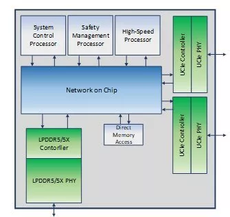
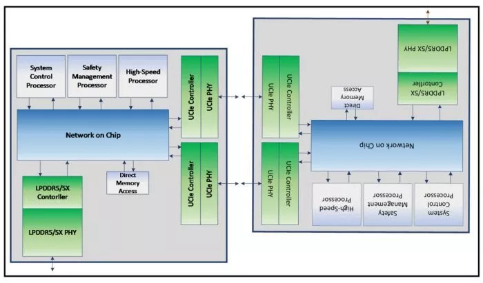
The SSG team of expert engineers and designers, dedicated to pushing the boundaries of semiconductor technology, has reached an extraordinary milestone with the prototype design of the industry's first system chiplet. This innovative chiplet, featuring the Cadence Chiplet Architecture and Framework, was developed in collaboration with the Cadence Design Services teams. The chiplet showcases the integration of processors, system IP, and memory IP, enabling multiple chiplets within the same package, interconnected using the UCIe standard interface. This chiplet includes a system processor, a safety management processor, Cadence controllers and PHY IP for LPDDR5 and UCIe, and the Cadence Janus NoC technology. It also serves as a dynamic platform to demonstrate Cadence's latest UCIe IP, boasting up to 64GB/s peak bandwidth, and LPDDR5 IP, offering up to 32GB/s peak memory bandwidth. This innovation sets a new industry benchmark and paves the way for Cadence to help our customers achieve cutting-edge advancements.

Figure 1: System chiplet

Figure 2: Integration of two system chiplets on the same package
Partnering with the Arm Chiplet Ecosystem
Cadence and Arm have a long-standing relationship and collaborated to transform the chiplet ecosystem. In March 2024, we announced a collaboration to deliver a chiplet-based reference design and a cutting-edge software development platform. This collaboration harnesses the innovative strengths of both companies, combining Cadence's robust IP and EDA solutions with Arm's state-of-the-art IP technologies. By leveraging learnings from the Arm chiplet ecosystem, Cadence is poised to significantly reduce design complexity and accelerate time to market for our customers. This collaboration pushes the boundaries of our chiplet solutions and provides our customers with a comprehensive and efficient development platform, empowering them to bring their products to market faster and with unprecedented performance.
This exciting announcement marks a significant step on our journey toward delivering a full chiplet reference design. As we continue to innovate and push the boundaries of technology, this collaboration with Arm sets the stage for even greater advancements in the chiplet ecosystem. Our commitment to providing cutting-edge solutions and comprehensive development platforms will empower our customers to achieve unprecedented levels of performance and efficiency. Stay tuned as we move forward in this transformative journey, bringing the future of chiplet technology to life.
Innovative IP Technology
Cadence's SSG team leverages decades of expertise in IP and subsystem design to pioneer advanced design technologies. With architecture and design proficiency at its core, their strategy is centered on crafting high-value solutions that tackle customer challenges head-on. By abstracting common functionalities into chiplet IP, the group accelerates time to market, enabling customers to innovate swiftly. Utilizing its mastery in advanced packaging and interconnect technologies, the SSG team develops scalable, high-performance technologies that empower customers to enhance efficiency and drive innovation.
The Importance of Chiplets
The industry is shifting from monolithic heterogeneous SoCs to chiplet-based products for several compelling reasons. Chiplet-based products enhance design and product factors, such as design/die reuse, contributing to engineering efficiency, faster platform refresh cadence, and the ability to optimize power, performance, and area (PPA) per chiplet. The rising cost of advanced process nodes raises the question of whether all components of an SoC product need to migrate to the latest node.
Chiplets offer a solution by enabling a multi-foundry business model and integrating cross-foundry process technologies within the same package. In addition, as technology density scaling slows in advanced nodes, designs are hitting Moore's law limits, requiring larger designs/chips with more functions and IP integrated into them, which are hitting process reticle limits. This shift is further supported by new packaging and interconnect solutions, such as advancements in 2.5D and 3D packaging and the standardization of Die2Die interfaces (e.g., UCIe). Chiplets are crucial for customers as they provide a transformative approach to addressing design challenges and accelerating time to market.
Conclusion
Cadence's advancements in chiplet technology mark a pivotal moment in the semiconductor industry. By leveraging innovative architectures, robust IP, and strategic collaborations with industry leaders like Arm, Cadence is setting new benchmarks for efficiency, scalability, and performance. These groundbreaking developments not only address the evolving needs of high-performance computing, automotive, and data center industries but also empower customers to overcome design challenges and accelerate their time to market. As we continue to push the boundaries of technology, Cadence remains committed to delivering cutting-edge solutions that drive innovation and shape the future of the chiplet ecosystem. Stay tuned for more exciting developments as we embark on this transformative journey.
Learn more about how Cadence's chiplets can benefit your business.
Related Semiconductor IP
- LPDDR5T / LPDDR5X / LPDDR5 Controller
- LPDDR5 Controller - Validates memory controllers for high-speed, power-efficient performance
- LPDDR5 IP solution
- Simulation VIP for LPDDR5
- LPDDR5 Synthesizable Transactor
Related Blogs
- Serial Wire Debug (SWD) Protocol: Efficient Debug Interface for Arm-Based System
- Cadence Commits to Join imec Automotive Chiplet Programme
- AMBA LTI Verification IP for Arm System MMU
- Accelerate Automotive System Design with Cadence AI-Driven DSPs
Latest Blogs
- Area, Pipelining, Integration: A Comparison of SHA-2 and SHA-3 for embedded Systems.
- Why Your Next Smartphone Needs Micro-Cooling
- Teaching AI Agents to Speak Hardware
- SOCAMM: Modernizing Data Center Memory with LPDDR6/5X
- Bridging the Gap: Why eFPGA Integration is a Managed Reality, Not a Schedule Risk
