Serial Wire Debug (SWD) Protocol: Efficient Debug Interface for Arm-Based System
Modern embedded systems are becoming increasingly compact, power efficient, and feature rich. As SoCs integrate more functionality, developers need reliable debug access without increasing pin count or board complexity. Serial Wire Debug (SWD) addresses these needs by providing a streamlined alternative to JTAG, enabling high performance debug features using only two pins, making it ideal for today’s constrained IoT, consumer, and automotive designs.
Overview of the SWD Protocol
The Serial Wire Debug (SWD) protocol is a compact, two-pin debug interface designed for Arm processor-based systems. As an alternative to the traditional JTAG interface, SWD provides efficient access to debug and trace features while minimizing pin count—a critical requirement for resource-constrained embedded and mobile devices.
SWD is widely adopted in Arm Cortex-M processor-based systems and is defined in the Arm Debug Interface Architecture Specification. The protocol enables debuggers to communicate with the Debug Access Port (DAP), facilitating operations such as memory access, register reads/writes, and system control through a minimal two-wire interface.
SWD Protocol Architecture
The SWD interface operates using only two signals:
- SWCLK (Serial Wire Clock): Clock signal driven by the debug host (master)
- SWDIO (Serial Wire Data I/O): Bidirectional data line shared between host and target
This simplified interface significantly reduces the pin overhead compared to JTAG's five-pin requirement, making SWD ideal for space-constrained designs.
Performance Advantages
SWD can achieve higher performance than traditional JTAG interfaces. The protocol uses the full clock cycle for data transfer (rising edge to rising edge), whereas JTAG drives data on the falling edge and samples on the rising edge. This enables SWD to operate at up to twice the frequency of JTAG in the same technology, providing faster debug access and reduced development time.
Key Protocol Features
1. The SWD protocol uses a point to point master–slave architecture where the debug host fully controls communication with a single target device via DP and AP registers.
2. Each transaction follows a defined sequence of request, acknowledge, and data phases, with LSB first transmission, explicit status responses (OK/WAIT/FAULT), and parity checking for reliability.
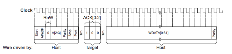
Image Reference: Courtesy of ARM® Debug Interface Architecture Specification ADIv6.0 (Figure B4-1 SWD successful write operation)
3. A configurable turnaround period ensures safe bidirectional control of the SWDIO line, while defined state transitions and idle cycles manage operation modes, protocol switching, and low power states
Protocol Error Handling
The SWD protocol includes strong error handling through
1. Even parity checks on both request and data phases to detect transmission errors.
2. Protocol errors such as invalid start, parity, stop, or park bits result in no target response, allowing the debugger to recognize the fault.
3. A defined line reset sequence—holding SWDIO high for at least 50 clock cycles followed by idle cycles—ensures reliable recovery and re synchronization of the interface.
Cadence SWD Verification IP Solution
Cadence AMBA SWD Verification IP offers a full featured solution for verifying SWD interfaces at both unit and system levels, supporting active, passive, and low power (dormant) configurations. It provides exhaustive protocol compliance checking, including reset sequences, turnaround timing, parity, ACK responses, idle cycles, and state transitions across SWD, JTAG, and Dormant modes. Advanced capabilities such as timing configurability, glitch detection, error injection, and functional coverage are combined with easy UVM/SystemVerilog integration and flexible runtime control for efficient debug and verification.
Cadence SWD VIP accelerates verification closure by providing:
- Ready-to-use building block sequences for common debug operations
- Automated protocol compliance checking
- Extensive coverage models aligned with ADI v6.0 specification
- Support for back-to-back VIP configurations for standalone testing
Whether verifying a custom SWD implementation, integrating debug infrastructure into a SoC, or validating system-level debug scenarios, Cadence SWD VIP provides the comprehensive toolset needed for efficient, thorough verification.
For any additional clarification or technical assistance, users are encouraged to reach out through talk_to_vip_expert@cadence.com
For more information, please visit https://www.cadence.com/en_US/home/tools/system-design-and-verification/verification-ip/simulation-vip/amba.html#amba-swd
Related Semiconductor IP
Related Blogs
- Accelerate Debug Productivity of Complex Serial Protocols
- Accelerate Debug Productivity of Complex Serial Protocols
- Tech Note: Use this Flexible and Efficient AC’97 IP Core for Simple Audio Interfaces and Legacy System Upgrades
- Overcoming the Protocol Debug Challenge