IP for TSMC
Welcome to the ultimate
IP
for
TSMC
hub! Explore our vast directory of
IP
for
TSMC
All offers in
IP
for
TSMC
Filter
Compare
510
IP
for
TSMC
from
41
vendors
(1
-
10)
Filter:
- 28nm
-
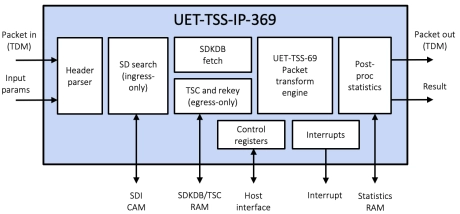
Multi-channel Ultra Ethernet TSS Complete Layer
- The UET-TSS-IP-369 (EIP-369) is an inline, high-performance, multi-channel packet engine that provides the complete TSS layer, bypass/drop and basic crypto processing at rates up to 1.6Tbps.
- The engine is designed for integration into the systems that require TSS processing for one or more ports. The engine is provided as separate ingress and egress data paths.
- The EIP-369 embeds the UET-TSS-IP-69 for the packet transformation.
-
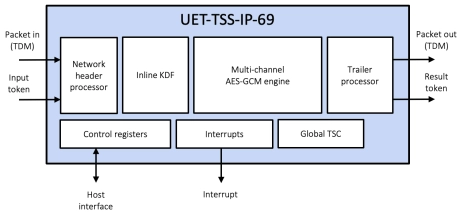
Multi-channel Ultra Ethernet TSS Transform Engine
- The UET-TSS-IP-69 (EIP-69) is a high-performance, multi-channel transform engine that provides the complete TSS packet transformation (including KDF and IP/UDP updates), bypass/drop and basic crypto processing at rates up to 1.6Tbps.
- The engine is designed for integration into the systems that require TSS processing for one or more ports. The engine is provided as separate ingress and egress data paths.
-
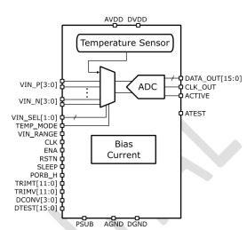
Ultra high-performance low-power ADC
- TSMC 28nm
- Ultra high-performance low-power ADC
- 12-bit ADC resolution
- Sampling rate up to 5GSPS
-
1.7GHz Multiplying PLL on TSMC 28nm
- Including Loop-filter
- VCO operating range : 850MHz - 1700 MHz
- Output frequency range : 850MHz -1700 MHz
- Input frequency range : 9.6MHz - 216MHz
-
5GHz Multiplying PLL on TSMC 28nm
- Including Loop-filter
- VCO operating range : 2500MHz - 5000 MHz
- Output frequency range : 1250MHz - 2500 MHz
- Input frequency range : 12MHz - 320 MHz
-
1.8GHz SSCG PLL on TSMC 28nm HPC+
- Including Loop-filter
- VCO operating range : 900MHz - 1800 MHz
- Output frequency range : 900MHz-1800 MHz
- Input frequency range : 12MHz - 192MHz
-
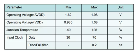
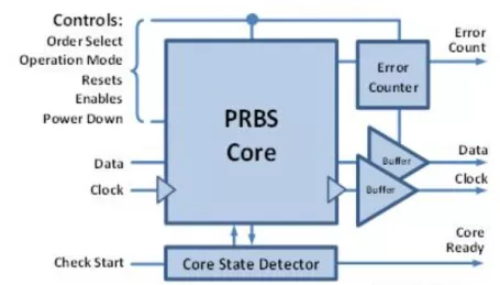
32Gbps, 31 order, Pseudo Random Bit Sequence Generator / Checker
- This unit generates and checks Pseudo Random Bit Sequence (PRBS) of 31 order, up to 32Gbps. Error count is accurate: no double counts or omissions regardless of error sequence or frequency of occurrence.
- Can be used as Generator, Checker or both. No inductors are used minimizing area and EM interference. Simple control interface, with low frequency asynchronous signals only.

-
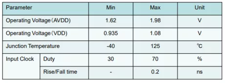
32Gbps, 7/15/31 order, Pseudo Random Bit Sequence Generator/Checker
- PRBS order: 7, 15 or 31 based on formulas: X1=X6^X7; X1=X14^X15; X1=X28^X31
- Full bit rate at input and output up to 32Gbps
- Generator, Checker and Counter functions
- Accurate error count: no omissions or double counts
- Full rate CMOS differential input data, centered with half-rate CMOS differential clock
- Full rate CMOS differential output data, aligned with half-rate CMOS differential clock
-
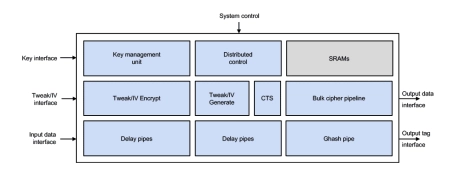
Fast Inline Cipher Engine, AES-XTS/GCM, SM4-XTS/GCM, DPA
- One input word per clock without any backpressure
- Design can switch stream, algorithm, mode, key and/or direction every clock cycle
- GCM: throughput is solely determined by the data width, data alignment and clock frequency
- XTS: block processing rate may be limited by the number of configured tweak encryption & CTS cores; a configuration allowing 1 block/clock is available
-
Ultra-Low-Power Temperature/Voltage Monitor in 28nm CMOS
- The ODT-TVM-ULP-001C-28 is an ultra-low power temperature and voltage monitor designed in a 28nm standard CMOS process.
- This IP operates over the entire temperature range of -40°C to 150°C.
- The temperature monitor achieves ±4C temperature accuracy without trim and ±1C temperature accuracy after a single room temperature trim.