Memory & Libraries IP for TSMC
Welcome to the ultimate
Memory & Libraries IP
for
TSMC
hub! Explore our vast directory of
Memory & Libraries IP
for
TSMC
All offers in
Memory & Libraries IP
for
TSMC
Filter
Compare
48
Memory & Libraries IP
for
TSMC
from
13
vendors
(1
-
10)
Filter:
- 28nm
-
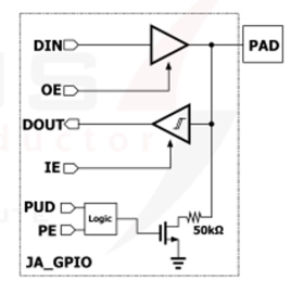
1.2V Thin Oxide GPIO on TSMC 28nm RF HPC+
- The 1.2V Thin Gate GPIO is an IP macro for on-chip integration. It is a 1.2V general purpose I/O that does not rely on thick-gate devices. Only thin-gate, 0.9V capable core MOS devices are used in the design.
- Supported features include core isolation, programmable slew rate compensation, programmable drive strength, input/output enable, pull select and pull enable. Extra features such as programmable hysteresis can be supported upon request.
-
3.3V Capable GPIO on TSMC 28nm RF HPC+
- The 3.3V capable GPIO is an IP macro for on-chip integration. It is a 3.3V general purpose I/O built with a stack of 1.8V thick oxide MOS devices. It is controlled by 0.9V (core) signals.
- Supported features include core isolation, output enable and pull enable. Extra features such as input enable/disable, programmable drive strength and pull select, can be supported upon request.
-
1.8V Capable GPIO on Samsung Foundry 4nm FinFET
- The 1.8V capable GPIO is an IP macro for on-chip integration. It is a 1.8V general purpose I/O built with a stack of 1.2V MOS FINFET devices. It is controlled by 0.75V (core) signals.
- Supported features include core isolation, output enable and pull enable. Extra features such as input enable/disable, programmable drive strength and pull select, can be supported upon request.
-
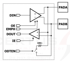
LVDS Transceiver in TSMC 28nm
- This 1.8V LVDS transceiver, designed for TSMCs 28nm process, delivers high-speed, low-power differential signaling with superior signal integrity.
- Engineered with 1.8V thick oxide devices and a 0.8V standard core interface, it operates ef- ficiently across a wide temperature range (-40°C to 125°C).
-
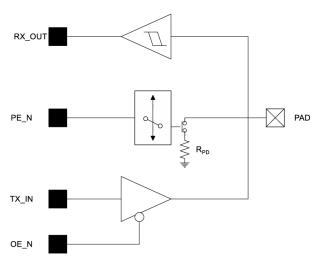
1.8V/3.3V Multi-Voltage GPIO in TSMC 28nm
- This silicon-proven TSMC 28nm Digital I/O Library delivers a high-performance, low-power interface solution designed for advanced digital applications.
- Featuring a triple-staggered architecture, this versatile library supports multi-voltage and multi-protocol GPIO, ensuring seamless integration across diverse system requirements.
-
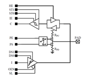
1.8V/3.3V Switchable GPIO in TSMC 28nm
- A TSMC 28nm Wirebond I/O Library with a switchable 1.8V/3.3V GPIO, with Specialized RF Wirebond Cells for LNAs.
- A key attribute of this silicon-proven, inline library is to detect and adjust to a VDDIO supply of 1.8V or 3.3V during system operation.
- The GPIO can be configured as input, output, open-source, or open-drain with an optional 60kohm pull-up or pull-down resistor.

-
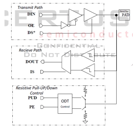
ESD Solutions for Multi-Gigabit SerDes in TSMC 28nm
- A Wirebond and FlipChip compatible <80fF ESD Solutions for Multi-Gigabit SerDes Applications.
- This silicon-proven TSMC 28nm Digital I/O Library delivers a low-capacitance, high-reliability interface solution optimized for advanced semiconductor applications.
- Featuring low-capacitance LVDS differential pairs (<250fF per pin) at 0.8V, this library ensures superior signal integrity for high-speed applications.
-
High-Speed 3.3V I/O library with 8kV ESD Protection in TSPCo 65nm
- A 3.3V wirebond I/O library with 8kV HBM ESD protection, a 1.2Gbps LVDS, GPIO, and I2C compliant ODIO in an ultra-small footprint.
- This library ensures robust reliability in challenging environments, with capabilities including 8kV HBM, 500V CDM, and a robust 2kV IEC 61000-4-2 system stress capability.
- Its compact footprint makes it ideal for applications where size is critical.
-
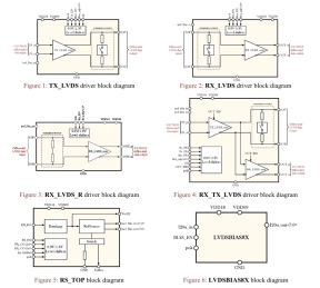
1.25 Gbps LVDS IPs library
- TSMC 28nm CMOS
- TIA/EIA-644 LVDS standards without hysteresis
- Data transfer rate: 1250Mbps
- 1.8V IO voltage supply
-
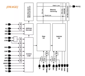
eTCAM (Embedded Ternary Content Addressable Memory IP
- One cycle operation latency (without priority encoder)
- Valid Bit per entry to reduce power
- Valid Bit reset in one cycle support
- Mask input option for bit-write and masked search key