Interface IP Cores for TSMC
- 28nm
-
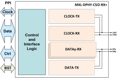
MIPI D-PHY RX+ (Receiver) IP
- The MIPI® D-PHY RX+ is a proprietary implementation of the MIPI Camera Serial Interface 2 (CSI-2) and Display Serial Interface (DSI) D-PHY Receiver.
- It is optimized to achieve full-speed production testing, in-system testing, and higher performance compared to traditional configurations, while reducing area and standby power.
-
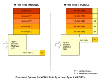
MIPI M-PHY IP
- The MIPI M-PHY is a high-frequency low-power, Physical Layer IP that supports the MIPI® Alliance Standard for M-PHY.
- The IP can be used as a physical layer for many applications, connecting flash memory-based storage, cameras and RF subsystems, and for providing chip-to-chip inter-processor communications (IPC).
-
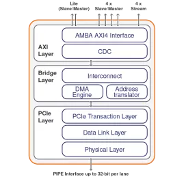
PCIe 3.1 Controller with AXI
- Compliant with the PCI Express 3.1/3.0, and PIPE (16- and 32-bit) specifications
- Compliant with PCI-SIG Single-Root I/O Virtualization (SR-IOV) Specification
- Supports Endpoint, Root-Port, Dual-mode configurations
- Supports x16, x8, x4, x2, x1 at 8 GT/s, 5 GT/s, 2.5 GT/s speeds
- Supports AER, ECRC, ECC, MSI, MSI-X, Multi-function, P2P, crosslink, and other optional features
- Supports many ECNs including LTR, L1 PM substates, etc.
-
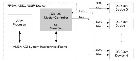
I2C Controller IP – Master, Parameterized FIFO, AXI Bus
- The DB-I2C-M-AXI Controller IP Core interfaces an ARM, MIPS, PowerPC, ARC or other high performance microprocessor via the AMBA 2.0 AXI System Interconnect Fabric to an I2C Bus. The I2C is a two-wire bidirectional interface standard (SCL is Clock, SDA is Data) for transfer of bytes of information between two or more compliant I2C devices, typically with a microprocessor behind the master controller and one or more slave devices.
- The DB-I2C-M-AXI is a Master I2C Controller that controls the Transmit or Receive of data to or from slave I2C devices. Figure 1 depicts the system view of the DB-I2C-M AXI Controller IP Core embedded within an integrated circuit device.
-
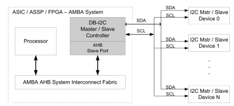
I2C Controller IP- Master / Slave, Parameterized FIFO, AHB Bus
-
The DB-I2C-MS-AHB Controller IP Core interfaces a microprocessor via the AMBA AHB Bus to an I2C Bus in Standard-Mode (100 Kbit/s) / Fast-Mode (400 Kbit/s) / Fast-Mode Plus (1 Mbit/s) / Hs-Mode (3.4+ Mb/s) / Ultra Fast-Mode (5 mbit/s).
The I2C is a two-wire bidirectional interface standard (SCL is Clock, SDA is Data) for transfer of bytes of information between two or more compliant I2C devices, typically with a microprocessor behind the master controller and one or more slave devices.
The DB-I2C-MS-AHB is a Master / Slave I2C Controller that in Master Mode controls the Transmit or Receive of data to or from slave I2C devices while in Slave Mode allows an external I2C Master device to control the Transmit or Receive of data.
-
-
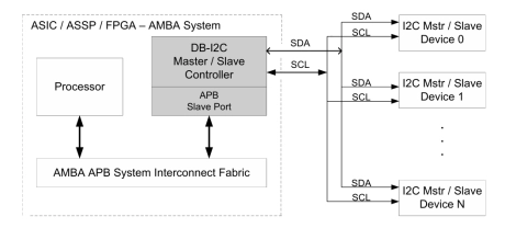
I2C Controller IP- Master / Slave, Parameterized FIFO, APB Bus
-
The Digital Blocks DB-I2C-MS-APB Controller IP Core interfaces a microprocessor via the AMBA APB Bus to an I2C Bus in Standard-Mode (100 Kbit/s) / Fast-Mode (400 Kbit/s) / Fast-Mode Plus (1 Mbit/s) / Hs-Mode (3.4+ Mb/s) / Ultra Fast-Mode (5 mbit/s).
The I2C is a two-wire bidirectional interface standard (SCL is Clock, SDA is Data) for transfer of bytes of information between two or more compliant I2C devices, typically with a microprocessor behind the master controller and one or more slave devices.
The DB-I2C-MS-APB is a Master/Slave I2C Controller that in Master Mode controls the Transmit or Receive of data to or from slave I2C devices while in Slave Mode allows an external I2C Master device to control the Transmit or Receive of data.
-
-
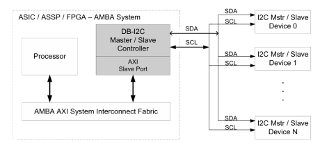
I2C Controller IP- Master / Slave, Parameterized FIFO, AXI Bus
- The DB-I2C-MS-AXI Controller IP Core interfaces a microprocessor via the AMBA AXI Bus to an I2C Bus in Standard-Mode (100 Kbit/s) / Fast-Mode (400 Kbit/s) / Fast-Mode Plus (1 Mbit/s) / Hs-Mode (3.4+ Mb/s) / Ultra Fast-Mode (5 mbit/s).
- The I2C is a two-wire bidirectional interface standard (SCL is Clock, SDA is Data) for transfer of bytes of information between two or more compliant I2C devices, typically with a microprocessor behind the master controller and one or more slave devices.
- The DB-I2C-MS-AXI is a Master / Slave I2C Controller that in Master Mode controls the Transmit or Receive of data to or from slave I2C devices while in Slave Mode allows an external I2C Master device to control the Transmit or Receive of data.
-
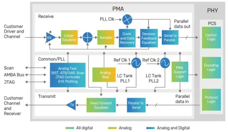
Programmable PCIe2/SATA3 SERDES PHY on TSMC CLN28HPC
- Programmable SERDES analog front end that supports 1 to 6+ Gbps standard serial protocols
- Compact form factor – 0.116 mm2 active silicon area per lane including ESD
- Industry leading low power – typically 6.3 mW/Gbps (@6Gbps) including termination
- Minimal latency – 3 UI between parallel transfer and serial transmission
-
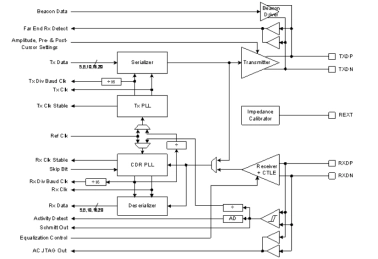
10Gbps Multi-Protocol PHY IP (+PCIe 3.1)
- Supports 10G-KR, PCIe 3.1/2.0/1.0, XAUI, Q/SGMII, and Gigabit Ethernet
- LC tank PLL with a wide range of reference clock frequencies and SSC
- High-performance decision feedback equalization and adaptive CTLE
- Serial and parallel loop-back functions
- Available in X1 through X10 lane configurations
-
USB 2.0 picoPHY - TSMC 28LPP18 x1, North/South (vertical) poly orientation
- Ported to over 50 different processes and configurations ranging from 65-nm to 14/16-nm FinFET
- Supports the USB 2.0 protocol and data rate (480 Mbps)
- Supports the USB Type-C specification
- USB femtoPHY, USB nanoPHY and USB picoPHY offer a tunability feature that allows quick, post-silicon adjustments that occur due to process variations, or unexpected chip and board parasitic, without modifying the existing design