Memory Controller/PHY IP for TSMC
Welcome to the ultimate
Memory Controller/PHY IP
for
TSMC
hub! Explore our vast directory of
Memory Controller/PHY IP
for
TSMC
All offers in
Memory Controller/PHY IP
for
TSMC
Filter
Compare
65
Memory Controller/PHY IP
for
TSMC
from
8
vendors
(1
-
10)
Filter:
- 28nm
-
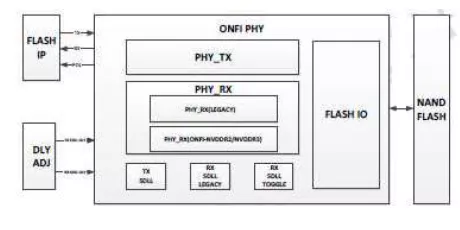
ONFi PHY 4.0 (FPHY+MDLL+SDLL Regulator) (Silicon Proven in TSMC 28HPC+)
- Support ONFi 4.0 IO Electrical Specification
- Support Legacy up to 50MHz
- Support NV-DDR2 with operating frequency up to 533Mbps
- Support NV-DDR3 with operating frequency up to 800Mbps
-
M31 eMMC/SDIO at TSMC 28HPC+ Process
- Supports HS400 (400Mbps), HS200 (200Mbps), High-speed DDR (52Mbps) and etc.
- Consisting of driver, receiver & pull-up/down resistors
- Power-sequence free
- Provides multi-driving-strength selection
-
SD/eMMC - TSMC 28HPM, North/South Poly Orientation
- Compliant with eMMC 5.1 HS400, SD 6.0 SDR104, DDR50, JESD8-7a (1.2V/1.8V) and JESD8c.01 (3.3V)
- Fully integrated hard macro with high speed IOs and DLL/delay lines
- Fine resolution DLL/delay lines for HS400 strobe and HS200/SDR104 auto-tuning
- Easy to integrate with the highly optimized Synopsys SD/eMMC Host Controller IP, providing a complete low risk solution
-
SD/eMMC - TSMC 28HPCP, North/South Poly Orientation
- Compliant with eMMC 5.1 HS400, SD 6.0 SDR104, DDR50, JESD8-7a (1.2V/1.8V) and JESD8c.01 (3.3V)
- Fully integrated hard macro with high speed IOs and DLL/delay lines
- Fine resolution DLL/delay lines for HS400 strobe and HS200/SDR104 auto-tuning
- Easy to integrate with the highly optimized Synopsys SD/eMMC Host Controller IP, providing a complete low risk solution

-
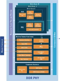
DDR4 multiPHY - TSMC 28HPC+18
- Support for JEDEC standard DDR4, DDR3, LPDDR2, and LPDDR3 SDRAMs
- Scalable architecture that supports data rates up to DDR4-2667
- Support for DIMMs
- Delivery of product as a hardened mixed-signal macrocell component allows precise control of timing critical delay and skew paths

-
LPDDR4 multiPHY V2 - TSMC28HPC+18
- Supports JEDEC standard LPDDR4X, LPDDR4, LPDDR3, DDR4, DDR3, and DDR3L (1.35V DDR3) SDRAMs
- Support for data rates up to 4,267 Mbps (process dependent)
- Designed for rapid integration with Synopsys Enhanced Universal DDR Memory/Protocol Controllers (uMCTL2/uPCTL2) for a complete DDR interface solution
- PHY independent, firmware-based training using an embedded calibration processor

-
ONFI IO v4.0, 800MT/s, TSMC 28HPC+, 1.8V, N/S orientation, H&V cell
- Supports ONFI 6.0(4.8Gbps), ONFI 5.1(3.6Gbps), ONFI 5.0(2.4Gbps), ONFI 4.1(1.2Gbps), ONFI 4.0(800Mbps) & ONFI 3.2(533Mbps)
- Power-sequence free
- Provides multi-driving-strength selection
- Provides CTT mode and LTT mode
-
TSMC CLN28LP 28nm LPDDR5 PHY - 3200Mbps
- Supports LPDDR5
- DFI 5.1 compliant
- Supports x4, x8 and x16 DRAMs
- Up to 72 bits wide and up to 4 ranks

-
TSMC CLN28LP 28nm LPDDR4 PHY - 2933Mbps
- Supports LPDDR4
- DFI 5.1 compliant
- Supports x4, x8 and x16 DRAMs
- Up to 72 bits wide and up to 4 ranks
-
TSMC CLN28LP 28nm LPDDR3 PHY - 2133Mbps
- Supports LPDDR3
- DFI 5.1 compliant
- Supports x4, x8 and x16 DRAMs
- Up to 72 bits wide and up to 4 ranks
