Types of Storages for Computing System-On-Chips
Priyank Shukla, Director, Analog Mixed Signal Design, Insilicorp
We are living in an age where we generate the same amount of data each year that has been generated since antiquity. Ever wondered how and where these peta /exa/zetta bytes of data are stored?
The story of large-scale data storage can be traced back to 1890 US census when punch cards – called electromechanical tabulating machines then, were used to record data. Herman Hollerith invented the recording of data on a medium that could then be read by a machine. Interestingly the design of punch cards was inspired by the way ticket conductors, back then, used to punch out the description of an individual, as light hair, dark eyes, large nose on a piece of a paper. A form of this practice is still prevalent in some public buses where bus conductor either punches or tears of edges of a ticket corresponding to the first and last stop and the time the ticket was bought.
During 1950s punch cards gave way to magnetic storage devices, when UNIVAC I, first commercial computer produced in the United States used tape drive as primary input-output (IO) device. These tape drives used a type of ferromagnetic material to store information readable to a computing and system and ruled the storage world until 1990s when optical disks replaced them for off-line data storage.
Incidentally, engineers in IC design still use a word “tape-out” that is remnant of this era of storage. The last day of IC design, even today is called tape-out day as it used to be the date when magnetic tapes with the recording of design data (GDSII) used to be sent out from a design house to a foundry for fabrication. Although today the GDSII is transferred over the internet and not through tapes to a foundry but the word tape-out still used.
The magnetic tapes, by design, provide limitation that the data can only be accessed sequentially. Hard disk drive (HDD) provided an alternative to overcome this limitation by employing a rotating disk to store information. Until 1990s floppy disks and until 2010s hard disk drives exploited the same principle for data storage. In both of the cases, the technology that replaced magnetic storage was electrically erasable programmable read-only memory EEPROM - also known as Flash.
HDDs were prevalent during personal computing explosion so most of the processor to storage interfaces used even today can trace their roots to HDD technology. Small Computer System Interface (SCSI) initially defined to standardize tape drive/HDD to processor interface evolved into Serial Attached SCSI (SAS) and Integrated Drive Electronics (IDE), later standardized under the name Advanced Technology Attachment (ATA) or sometimes referred as PATA (Parallel ATA) paved way for modern SATA (Serial Advanced Technology Attachment).
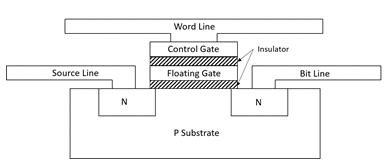
Toshiba developed and commercialized now ubiquitous flash memories in the 1980s. Flash memory stores information in an array of memory cells made from floating-gate transistors as shown below

A floating gate transistor is implemented by interposing an electrically isolated floating gate between the control gate and the MOSFET channel. As the floating gate is electrically isolated by its insulating layer, electrons placed on it are trapped until they are removed by another application of electric field and thus this structure acts as a single cell storage device.
The memory cells are classified based on the number of bits each cell stores. A single-level cell (SLC) device, stores only one bit of information per memory cell whereas a Multi-level cell (MLC) device offers the capability of storing more than one bit of information per memory cell. One popular example of MLC is Triple Level Cell (TLC) where each cell stores three bits of information.
With the evolution of process fabrication technologies, the channel length of floating gate transistor has reduced over the years allowing flash manufactures to pack more memory cells per unit area and produce denser storage devices over the years. However, with channel lengths reaching sub 10nm range, the industry realized, 3D integration is the only way forward to extend Moore’s law. Samsung shipped the world’s first 3D NAND device in 2013 and other vendors are following the suit. As of 2017, most Solid State Drives (SSD), a storage unit that uses ICs to store data, employ 3D TLC.
The two main types of flash memories prevalent today are called NAND and NOR flash. They are named such because the individual flash memory cells exhibit internal characteristics similar to respective logic gates. In a NOR flash when one of the word lines is pulled high, the corresponding storage transistor acts to pull the output bit line low whereas in a NAND flash several transistors are connected in series, and the bit line is pulled low only if all the word lines are pulled high.
Reading from NOR flash is similar to reading from random-access memory so NOR flash is used as RAM whereas NAND flash offers access of blocks of memories or pages and thus used as a storage device – an alternative to floppies and hard disks.
This NAND based flash memory is the basic storage unit of most of the storage devices today – right from a USB flash drive to Secure Digital (SD) card to eMMC or a data center SSD drive. A USB flash drive contains flash memory, its controller and USB interface on a PCB similar to an SD card that integrates flash memory and SD interface.
Handheld electronic devices such as digital cameras in pre-mobile phone era extensively used MMC (Multi Media Card), a commercial portable memory card standard used for solid-state storage, introduced by SanDisk and Siemens in 1997. MMC, however quickly gave way to SD that added security features to storage.
The mobile era popularized eMMC (embedded MMC) architecture that packs flash memory and its controller into a ball grid array package. Almost all mobile phones and tablets used eMMC for main storage up to 2015-17, when UFS (Universal Flash Storage) started to take control of the market.
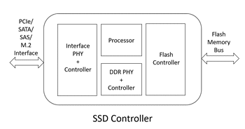
In the era of hyper-scale/cloud computing, distributed data centers, and enterprise storage, Solid State Drives (SSD) employing flash memory chips rapidly replaced disk/hard drives as they provide significantly faster and more reliable memory. Enterprise-class SSD consists of multiple flash memory chips with an SSD controller. The SSD controller not only spreads read and write operations over multiple memory chips but also ensures wear leveling, garbage collection, error detection, and correction. Below picture schematically presents an SSD controller.

The interface used to communicate with NAND Flash has been standardized by Open NAND Flash Interface (ONFI) workgroup. ONFI Standard not only defines the data rates and electrical parameters but also defines connector specification for NAND modules (similar to DRAM DIMMs).
New interface standards have been emerging since the invention of the first flash device by Fujio Masuoka in 1981 but the millions of terabytes the world creates every year and has since created are invariably stored in a flash storage with a floating gate MOSFET as basic storage unit!
Related Semiconductor IP
Related Articles
- Types of Memories in Computing System-On-Chips
- The rise of FPGA technology in High-Performance Computing
- Growing demand for high-speed data in consumer devices gives rise to new generation of low-end FPGAs
- Last-Time Buy Notifications For Your ASICs? How To Make the Most of It
Latest Articles
- An FPGA-Based SoC Architecture with a RISC-V Controller for Energy-Efficient Temporal-Coding Spiking Neural Networks
- Enabling RISC-V Vector Code Generation in MLIR through Custom xDSL Lowerings
- A Scalable Open-Source QEC System with Sub-Microsecond Decoding-Feedback Latency
- SNAP-V: A RISC-V SoC with Configurable Neuromorphic Acceleration for Small-Scale Spiking Neural Networks
- An FPGA Implementation of Displacement Vector Search for Intra Pattern Copy in JPEG XS