Accelerating SoC Evolution With NoC Innovations Using NoC Tiling for AI and Machine Learning
By Andy Nightingale, Arteris
A new trend is emerging in the design of high-end, multi-billion-transistor system-on-chip (SoC) devices. Referred to as “NoC tiling,” this evolutionary approach uses proven, robust network-on-chip (NoC) technology to facilitate scaling, condense design time, speed testing, and reduce risk.
Traditional NoC-Based SoC Design
NoCs are now employed in most of today’s leading SoCs. Traditional NoC-based SoC design commences by selecting a group of soft intellectual property (IP) cores, such as processors, accelerators, communications functions, memory, and more. Most of these soft IP cores are typically sourced from trusted third-party suppliers. This allows the design team to concentrate on developing their unique, proprietary IPs, which will set their SoC apart from competing products in the market.
All these soft IP cores are connected using a NoC, allowing each IP to transmit and receive packets of information from other IPs, including those communicating with the outside world. The interface to an IP is known as a socket. A network interface unit (NIU) connects an IP socket to the NoC and represents one of the most complex elements in the NoC structure.
The term “soft” in this context refers to the fact that the IPs, the NoC(s), and the NIUs are presented at the register transfer level (RTL). Eventually, a logic synthesis engine will process the entire SoC design. The resulting gate-level netlist will be handed over to the physical layout team for placement and routing.
Figure 1 shows a simplified view of this traditional implementation approach. The NoC demonstrated in this illustration reflects a generic topology. Common NoC topologies employed in SoCs include stars, rings, trees, hierarchical trees, meshes, or combinations.
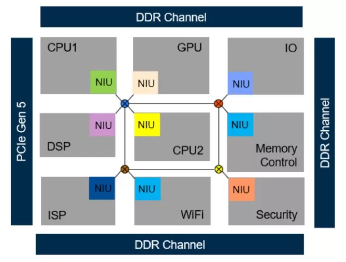
Figure 1: Simplified representation of a soft-IP and NoC-based SoC. (Source: Arteris)
Multiple packets can be in flight through the NoC simultaneously. The NoC will include buffers to store packets temporarily, switches to guide packets between initiator IPs and target IPs, and pipeline stages to help the physical layout team close timing.
Arrays of Homogeneous Accelerators
The generic SoC architecture reflected in Figure 1 may be assumed to be composed of many heterogeneous (assorted, diverse, and unrelated) IP functions. However, this architecture needs to be better suited to satisfy the exponentially increasing demand for SoCs that can perform tasks like artificial intelligence (AI) and machine learning (ML) with high performance, efficiency, and low power consumption.
A common architecture for SoCs intended for AI/ML applications is to combine an array of homogeneous (identical, standardized, and uniform) AI/ML accelerators with heterogeneous IP functions, as illustrated in Figure 2. Each AI accelerator is termed a processing element (PE), and a mesh NoC topology provides a widespread underlying communication infrastructure.
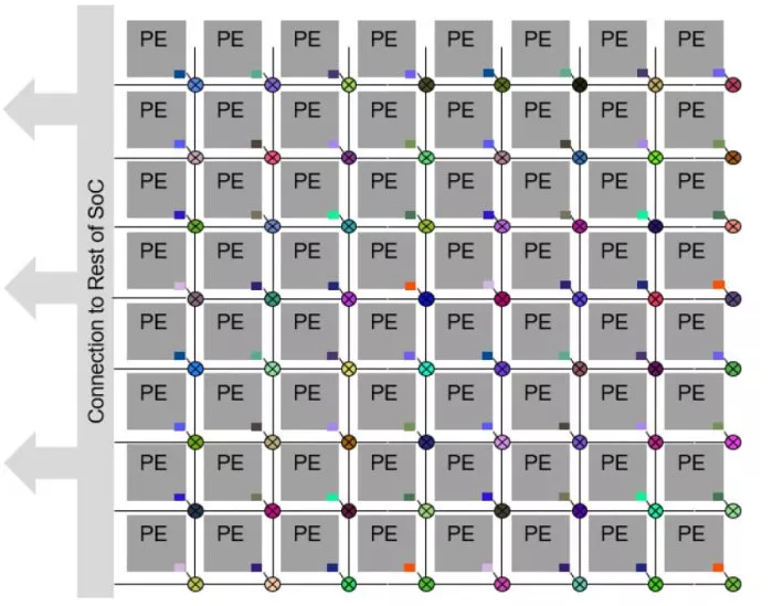
Figure 2: Many modern designs feature an array of accelerators. (Source: Arteris)
Each AI accelerator (PE) is connected to the mesh NoC by NIUs shown in different-colored square boxes, allowing them to exchange data seamlessly and collaborate in the AI/ML processing workflow.
In this case, each accelerator is presented as a hierarchical functional block. These identical blocks may contain multiple IPs and one or more internal NoCs. The main point is that this technique is still based on the traditional implementation approach in that each PE block needs an NIU configured individually.
NoC Tiling
The emerging trend mentioned at the beginning of this column is “NoC Tiling”, which allows SoC architects to more easily create scalable and modular designs by replicating NoC network interface units (NIUs) and their associated processing elements (PE). This enables faster innovation and more reliable, efficient AI chip development, as depicted in Figure 3.
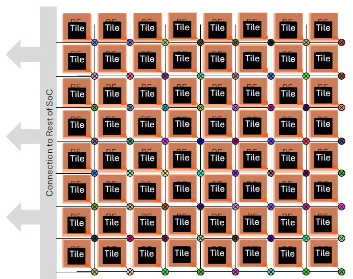
Figure 3: Mesh NoC with tiled NIUs. (Source: Arteris)
This approach allows the SoC architect to configure only one NIU and PE pair and then instantiate them multiple times. The ID of each tile is assigned after reset, using top-level signal tie-offs to overcome the fact that each tile is otherwise identical.
The mesh tiling approach is applicable to both non-coherent and coherent NoCs. Figure 4 shows a coherent NoC with multiple CPU tiles. Each tile could either be a single CPU or itself a cluster of CPUs. Each blue CPU tile is identical and replicated, the I/O tiles could be replicated too if desired. Together they form the coherent NoC along with I/O coherent interfaces, marked ‘I/O’. To the left of the coherent NoC is a simplified view of a mesh NoC with tiling of PEs (A) such as described in Figure 3, and to the right is mesh NoC A’ which is identical to A except flipped on the horizontal axis, something that is enabled by the tiling approach. Thus, each tile of the non-coherent NoC has been replicated to make A, a flipped copy to make A’ and the CPU tile and I/O tiles replicated to make the coherent NoC mesh. The re-use of physical layout significantly reduces implementation schedules.
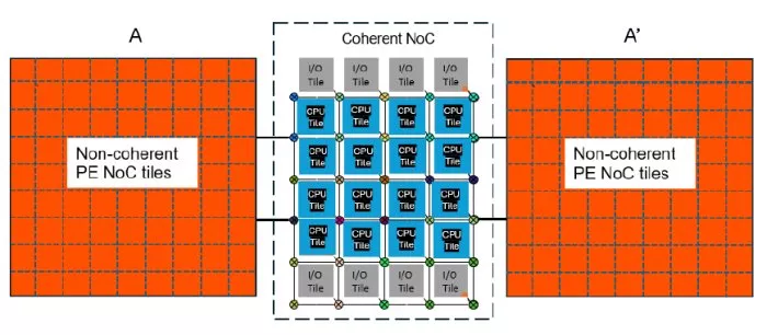
Figure 4: Coherent and non-coherent tiled NoCs
NoC-Enabled Tiling
Arteris is working with market-shaping leaders to address evolving IP and SoC design challenges. NoCs are one of the critical enablers of the emerging tiling implementation strategy. AI/ML SoC designs currently under development by Arteris customers are across the hottest vertical markets. This is illustrated in Figure 5, which reflects the AI application use cases by market.

Figure 5. AI use cases are present in key verticals today. (Source: Arteris)
Summary
Designing multi-billion-transistor SoCs is time-consuming and involves many challenges. Some SoC devices, such as those intended for AI/ML applications, may combine a group of heterogeneous IP functions with an array of homogeneous AI accelerators.
Using “NoC tiling” to easily create arrays of accelerators facilitates scaling, condenses design time, speeds testing, and reduces risk. As a next step, the accelerator array may even be incorporated into a “Chiplet tile,” which are physically separate silicon dies integrated into a single package to function as a unified system, offering greater flexibility with different technologies but involving more complex design and manufacturing compared to NoC tiles – but that’s a story for another day.
NoCs are critical enablers of current and emerging AI/ML application SoCs. Arteris is renowned for its industry-leading coherent and non-coherent NoC technologies. The company is dedicated to addressing evolving IP and SoC design challenges to propel the semiconductor industry forward.
About the author

Andy Nightingale, VP of product management and marketing at Arteris, has over 37 years of experience in the high-tech industry, including 23 years in various engineering and product management positions at Arm.
Related Semiconductor IP
- FlexNoC 5 Interconnect IP
- NoC System IP
- Non-Coherent Network-on-Chip (NOC)
- Coherent Network-on-Chip (NOC)
- High speed NoC (Network On-Chip) Interconnect IP
Related White Papers
- A novel 3D buffer memory for AI and machine learning
- Artificial Intelligence and Machine Learning based Image Processing
- Selection of FPGAs and GPUs for AI Based Applications
- An overview of Machine Learning pipeline and its importance
Latest White Papers
- Transition Fixes in 3nm Multi-Voltage SoC Design
- CXL Topology-Aware and Expander-Driven Prefetching: Unlocking SSD Performance
- Breaking the Memory Bandwidth Boundary. GDDR7 IP Design Challenges & Solutions
- Automating NoC Design to Tackle Rising SoC Complexity
- Memory Prefetching Evaluation of Scientific Applications on a Modern HPC Arm-Based Processor