eFPGA Creator GUI Tools Suite: A complete hardware and software infrastructure for creating customizable eFPGA IP blocks of Menta
Syed Zahid Ahmed, Alexandre Martheley, Laurent Rougé, Julien Eydoux, Jean-Baptiste Cuelle
Menta
Abstract
Increasing design complexity and high manufacturing costs have made industry reach at a point where it is almost essential to develop SoCs with some flexibility of post modification. The two most prominent members which are symbol of flexibility are Processors and FPGAs. Due to tough market pressures and stringent power challenges faced by industry it has become much interesting now compared to past to find a new marriage between SoCs and FPGAs in places where only SoC or FPGA stand alone independently can have tough challenge to meet requirements, this gives birth to embedded FPGAs (eFPGAs) for which Startup Menta® is playing a pioneering role to bring it to commercial level with industry standard tools to help semiconductor industry take benefits of FPGAs directly inside their SoCs in the form of customizable domain specific eFPGA IP block/blocks.
This paper presents a brief overview of new generation of Graphical tools suites we are developing to help our clients quickly and very easily obtain the customized eFPGA IP of their needs (Area, Power, Speed, I/Os, Target node etc.) this phenomenal benefit is hard to achieve with classical device based FPGAs.
1. Introduction
The increasing complexity of SoCs brings escalating design costs to semiconductor vendors. These costs are reaching a level where dedicated SoCs can no longer be designed for any and every application. They must instead be designed to be more flexible. In this way the high design costs can be amortized over several different end applications. Chips that can be used in multiple applications need a high degree of post-manufacturing configurability. This at present is achieved by many methods most prominent of them is by software using processors (ARM, MIPS…). Or on the other hand entire SoC is implemented on an FPGA fabric which has now become possible due to Moore’s law and strong development eco-system provided by FPGA Vendors (like Xilinx, Altera…).
However power consumption has become such a hot issue that even ASIC like solutions now have severe challenges to meet this issue. FPGAs are known to be very high in power consumption, High Area overhead and slower speeds. This raises a new challenge for Semiconductor industry. We require flexibility in our SoCs but due to power requirements we try to keep high end chips as custom as possible. The only element which provides significant post fabrication flexibility is processor with software. We believe it’s a right time we should start thinking about embedded FPGAs to bring salient FPGA benefits inside the SoCs to further augment the flexibility of processor only, by providing hardware upgradability in form of embedded FPGAs like software upgradability which exists currently with processors [1].
FPGAs are well known for their ease of programming in HDLs and standard well developed tools exist for their programming (including third party Synthesis like Synplicity® etc.). We at Menta realized the importance of this challenge and particular benefit of FPGAs that they are programmed with standard languages (VHDL/Verilog…). So the ASIC designer needs no extra burden of a language or a sub version of a language like is done with C/C++ in some emerging Processor/MPSoC solutions/startups to better optimize with their hardware utilization. This in many cases causes troubles and burden of an additional effort by the end user and they prefer to remain general purpose (like with ARM, MIPS…). We considered all these issues so the programming of eFPGA of Menta is like programming any classical FPGA. We use standard synthesis tools on front end and provide complete backend infrastructure of programming by proprietary tools (eFPGA Programmer) of Menta [2].
Having achieved that and in addition also analyzing and demonstrating the possibility of using ESL level programming on top of the standard tools flow [3] our next objective was to really take our customization capability to new levels for our customers. This paper is our first paper to provide brief introduction to the steps we are taking to achieve it.
For this challenge we identified two major issues by industrial observation. First our tools (eFPGA Programmer) should be fully adaptable and compatible with any customization we make in the architecture. We got inspiration for this from solutions like of Tensilica® (www.tensilica.com), Arc® (www.arc.com) etc. who provides configurable solutions based on consumer needs with complete software support, so the end user does not have to do additional efforts. In a similar fashion we designed and architected our eFPGA Programmer tools suite to be fully adaptable to any customization. So our client will get a complete software support instantly (transparent to the user) for any kind of customized eFPGA IP he will require for his target needs.
Second there should be a complete user friendly interactive graphical infrastructure to help our clients independently (basic solutions) or in close partnership (advanced solutions) with us explore and develop feasibilities of different solutions to find best suit of their needs. We see that a significant step ahead for both better serving our clients and pushing our product differentiation ahead.
The rest of the paper is organized as follows. In section 2 we will briefly provide an introduction to our eFPGA and programming flow. In section 3 we will describe fundamental concepts and motivations for GUIs, the FPGA designer tools suite flow and briefly discuss how we created them. In section 4 we will give a small example of generating an eFPGA IP using the tools flow to explain how easy it is for end user and what efforts we are doing in this regard and finally section 5 will present conclusions and future strategies and section 6 with references for further information.
2. eFPGA basics and its programming flow
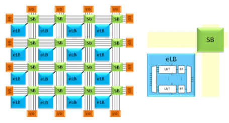
Fig. 1: eFPGA arch abstract view
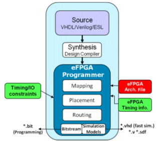
Fig. 2: eFPGA Programmer tool flow for programming eFPGA [2]
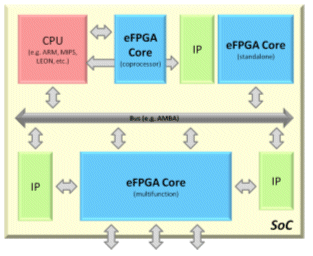
Fig. 3: eFPGAs in SoC (a concept diagram)
Figure 1 shows the abstract block diagram of Menta’s eFPGA. The type shown in figure is a homogeneous architecture with all elements of type eLB (embedded Logic Block) which is a cluster of LUTs. The eFPGA IP is highly customizable. It can be purely soft and technology independent (with no SRAM, pass transistors, tri state buffers etc.) or can be semi custom with some technology dependent cells like SRAM, or full custom. The details about the eFPGA are beyond the scope of this paper, they have been discussed in more detail in a datasheet [2]. The high level of generalness and technology independent soft IP concept of Menta which is embedded in the design theme of how we created our architecture provides the immense flexibility to target any process technology for fundamental architecture and using specific custom cells (SRAM, Memories etc.) of a specific process to further fine tune the design for target needs. This is a significant benefit for the user because the soft IP of eFPGA (HDL) can be ported immediately to any process node for experimentation and early test chips and finally for production a more custom solution can be created depending on target market needs.
Figure 2 describes the eFPGA Programmer tools suite [2] which is the programming tool flow of eFPGA. It uses Synopsys® DC™ (Design Compiler) on the front end which provides the power of synthesizing any application in VHDL/Verilog or mixed. Use of ESL for programming in ANSI C/C++ through Mentor’s Catapult™ has also been done and demonstrated in [3]. The synthesizer synthesizes the design and synthesized netlist (edif or verilog) is fed to back end of eFPGA Programmer for mapping, Place & Route and programming files generation. It also provides possibilities of verification at different steps [2]. The architectural and timing details of eFPGA are provided with architecture and timing files. Like the eFPGA hardware eFPGA Programmer is also built from ground up to be fully adaptable with any customization done in the architecture. This ensures complete hardware software adaptability for any needs of the end user. It is due to these co-adaptable properties of the hardware and software it was possible to create the entire tools suite infrastructure of FPGA designer which is discussed in next section on an abstract level.
Figure 3 gives the concept of eFPGA in a SoC to clearly identify that it’s a complete hardware block of FPGA which can be used inside a SoC like other IPs to provide several key features like Product differentiation, Fast time to market, reconfigurable acceleration, interfacing, interconnects and lot more (eFPGA can do all what FPGAs can do so its obvious!).
3. eFPGA Creator Tools Suite
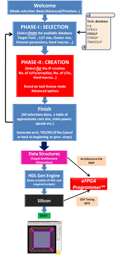
Fig. 4: eFPGA Creator flow
3.1 eFPGA Creator Flow
Figure 4 explains the flow of the eFPGA Creator tools suite. The description of the flow is straight forward and is self explanatory from the figure 4. In the beginning tool checks what kind of license of tool the user has obtained from Menta which will change the level of customization options the user will get. In first phase of tool the user selects the basic elements of his choice from the set of available options provided by Menta like process technology, LUT size, Routing strength and Hard Macros etc. (components like Hard Macro are technology dependent). In the next phase User chooses amount of resources needed for his application like number of LUTs, amount of I/Os, memory etc. For both Phase-I and Phase-II Menta can provide services to help the client make better decisions based on his target needs. It’s a close partnership work between Menta and the Client to better understand the requirements. After gathering all the required information the tool is ready to create all the data structures needed for creation of Architecture. Due to phase-I the tool already has approximate knowledge about silicon so at this step the FPGA designer gives an approximate hint about the expected area of core, static power, speeds of basic elements etc. This greatly helps to have an early feeling of results of the selected choices and make a fast design space exploration. The MAF (Menta Architecture File) file provides all the architecture information to eFPGA Programmer for performing the application mappings; Place and Route etc. (figure 2). The HDL generation engine generates all the HDL design files of the architecture with required scripts for silicon implementation. After implementation on the target silicon node the extracted timing information is fed back to eFPGA Programmer with MTF (Menta Timing File) which allows eFPGA Programmer to perform all the timing analysis of mapped application for optimizing critical paths and frequency calculations.
By the end of the flow of figure 4 the user has the GDSII of the desired architecture with complete software flow ready to map target applications on the designed customized FPGA. It greatly helps the users to fine tune their FPGA requirements and get a more optimal and customized solution which will better help to decrease the fundamental silicon gap between FPGAs and ASICS [4]. Thanks to the customization offered by our solutions.
3.2 eFPGA Creator GUIs
To achieve the real strength of figure 4 and make the whole process user friendly and professional it was essential to create graphical tools suite to perform all these tasks efficiently. For this first question and challenge was how to design that, what kind of tools to use for it? etc. The two main options we came up with after some analysis were Eclipse (http://www.eclipse.org/) and Qt (http://qt.nokia.com/). We found that Qt better serves our current and future roadmap requirements. It has also helped us develop all the tools in C++/C and make all our tools Platform Independent. Thanks to this advantage all the tools of Menta (Including eFPGA Programmer) can run on all platforms (Windows, Linux, Mac, Solaris).
Figure 5 shows the Integrated Design Suite of the FPGA designer (in Windows VISTA) with some of the tools running inside. In next section we will see with a basic example how simple and user friendly it is to create a customizable eFPGA block with these GUI tools.
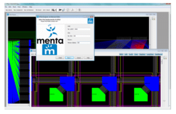
Fig. 5: FPGA generator Integrated Design Suite
4. Example of creating an eFPGA IP block
Figures 6 to 12 demonstrate some of the key steps of the flow of figure 4 in basic mode of the tool. Like figure 4 the figures are self explanatory and it can be seen how convenient it is to generate a customized IP blocks of eFPGA. Let’s discuss some key aspects of every step briefly.
The first major selection option is to choose the target node, based on that all next windows provides options with that node. In figure 6 it can be seen there are several target node options. We choose ST65nmLP process which is our current major focus and have widest options compared to other possible nodes.
Figure 7 follows our choice in figure 6 and can be seen that we have a list of basic building element of eFPGA (the Tile, which is the cluster of LUTs with SBOX). In the table it can be seen for every tile we can see the basic information like LUT size, routing strength etc. What is worth noticing here is the “Status” information. The parameters like Lut size, routing strength etc (advanced version of tool provides further deep details) help to customize the architecture based on target needs. The status information has got its inspiration roots from the well known five stage evaluation process of TSMC for IPs, basic blocks etc. It can be seen that we have seven steps (code name 7evenStar) for evaluation with few initial steps in addition to the higher five which are similar like TSMC. This will give a remarkable confidence to the end client about the choice he will make in selection. Our goal at Menta is to provide a wide variety of options in architecture along with as much as possible silicon confidence for the end client. The options which will be used most for wider range of application needs will gradually increase in their Star value and for those options the user will have a high yield confidence like the well known star IPs (ARM, Synopsys… etc.). We think through that we will have a significant competitive edge over any new comer trying to enter this area in addition to our continued architectural innovations. In the figure we selected the number three tile which is our current best general option and mentioned on our Data sheet [2]. Its ranking is higher and is about to be sent for Test Chip.
Figure 8 shows the selection of Hard Macro (in this case SRAM memory blocks) elements like the Tiles in previous step based on target needs. The Hard Macros are mostly from the FAB or 3rd Party providers. In our case we have all from ST through CMP [5]. In the table the basic details of the blocks can be seen and are usual and self explanatory. For current example we chose option 4 which is a 16kbit single port high density memory block.
At this step the tool knows all the blocks which will be used inside the eFPGA and figure 9 shows the first main window when we start describing our target needs. In figure we see the major demands; number of LUTs, I/O needs and amount of memory desired. It can be seen we demanded 2200 LUTs (LUT6 because we selected a LUT6 based Tile), 200 IOs and 170kbits of memory.
Figure 10 shows the feed back of the tool. The tool analyzed our demands based on architectural issues and proposes the nearest possible actual parameters. We see we have two nearest possibilities one little higher than demanded and the other way around. In this example case we took the smaller value which will give us 2116 LUT instead of 2200, 160kbit of memory compared to 170kbit. The IOs in both cases are already higher than demanded thanks to the nature of Menta’s IO control architecture.
Figure 11 shows the summary of the architectural parameters including some approximate idea about the silicon which is possible due to our 7evenStar evaluation. For all tiles with rank 2Star or higher we already have some silicon information to make approximate calculation. It can be noticed how helpful it is for design space exploration. If the end results are not matching with the user requirements he can try with different options like e.g. using higher speed elements with trade off of power or the other way around, or trying a different solution with increased hard macros etc.
Finally figure 12 provides a detailed graphical view generated by the tool with all elements to give a feeling how the IP will look like on Silicon. This detailed GUI will also help in eFPGA Programmer for analyzing the place and route like is done in the well known tools of Xilinx or Altera.
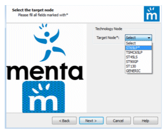
Fig. 6: Selection of target technology node
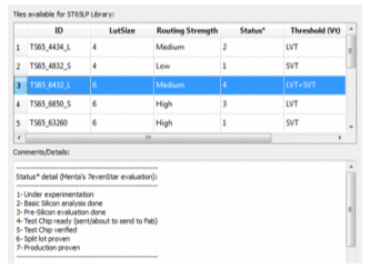
Fig. 7: Tile selection from the available library
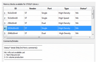
Fig. 8: Memory (Hard Macro) block selection from library
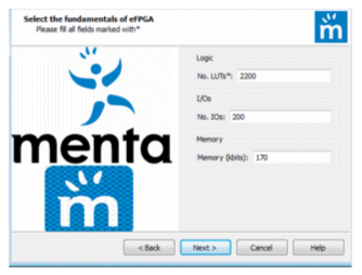
Fig. 9: Describing the desired parameters (logic, IOs, HM …)
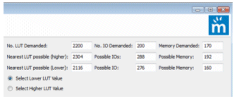
Fig. 10: Automatic feedback of the nearest actual resources possible
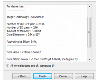
Fig. 11: Summary of the statistics of choices
By this simple example it can be seen how easy it is to create customizable IP blocks of our eFPGA using the FPGA designer tools suite. In the example we only showed the basic mode options, the advanced mode will allow stronger customization control over parameters to make further fine tuned IP block.
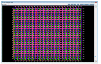
Fig. 12: The graphical view of the generated IP
5. Conclusions & Future works
In this paper we provided a brief introduction from the industrial perspective of the general motivation about eFPGAs, our philosophy with it and what inspired us to create FPGA designer tools suite. We provided a brief introduction to our technology in section 2 for the smooth reading flow of the paper for the reader without going in deep details which can be found in references. We introduced the flow of FPGA designer and explained its features and potentials. We briefly covered the GUIs, how we made them and why we chose to make them with Qt (of Nokia now). We gave a sample snapshot of the tool IDE to give a feeling of its potentials and ease of use. We gave a small example for the proof of concept of the tools. We briefly described the potentials with this example and showed what promising technical and commercial benefits these tools suits will open for Menta and our clients. We highlighted our seven step (7evenStar) evaluation process and discussed what benefits and potentials it can open for Menta and our clients.
Looking towards the future we see nothing but opportunities which will be enabled by these tools for both Menta and our clients. We will continue improving these tools and continuously enhance our technology database (figure 4) to provide more and more elements and options for our clients with also increasing the Star value of the components. At present our most comprehensive offerings are on 65nm ST process. We have demonstrated some results for ST90nm and ST45nm also [2]. All the technology access to ST is provided by CMP [5]. Recently we have started working on TSMC 65nm also through EuroPractice [6]. We will rapidly enhance our capabilities and offerings for TSMC process to better take leverage of strong market dominance of TSMC.
Notice of correction on 2 November 2010:
The article was published on D&R website on 1 November 2010, based on the article of Menta in IPESC09 from December 2009. Several things, tools flows and names changed over time and can change any time without notice. The article is slightly modified for the changed names without changing the contents and motivations which still holds. Following terms are modified: FPGA Designer to eFPGA Creator, eCB to eLB and Niagara to eFPGA Programmer.
Menta and D&R apologize readers for any inconvenience or confusion created about the tools names and products compared to 2010 Press releases of Menta.
Please visit www.menta.fr for the latest up to date products.
6. References
[1] IP08 Panel: SoC Configurability (www.design-reuse.com/ip08/program/panel_socconfigurability.html)
[2] Datasheet brief of eFPGA core of Menta (www.menta.fr/down/DatasheetBrief_eFPGA_Core.pdf)
[3] S Z Ahmed, J Eydoux, L Rougé, JB Cuelle, G Sassatelli, L Torres, "Exploration of power reduction and performance enhancement in LEON3 processor with ESL reprogrammable eFPGA in processor pipeline and as a co-processor", DATE-09
[4] I. Kuon and J. Rose, "Measuring the Gap between FPGAs and ASICs" IEEE Transactions on CAD of Integrated Circuits and Systems, Vol. 26, NO. 2, FEBRUARY 2007, pp. 203 - 215
[5] CMP (Circuits Multi-Projects): http://cmp.imag.fr
[6] EuroPractice : http://www.europractice-ic.com/
Related Semiconductor IP
- ReRAM NVM in DB HiTek 130nm BCD
- UFS 5.0 Host Controller IP
- PDM Receiver/PDM-to-PCM Converter
- Voltage and Temperature Sensor with integrated ADC - GlobalFoundries® 22FDX®
- 8MHz / 40MHz Pierce Oscillator - X-FAB XT018-0.18µm
Related Articles
- A tutorial on tools, techniques, and methodology to improve FPGA designer productivity
- FPGA Development Tools Qualification for ISO26262 - An Overview and guideline
- Partial reconfiguration in FPGA rapid prototyping tools
- Designers find tools, intellectual property wanting
Latest Articles
- An FPGA-Based SoC Architecture with a RISC-V Controller for Energy-Efficient Temporal-Coding Spiking Neural Networks
- Enabling RISC-V Vector Code Generation in MLIR through Custom xDSL Lowerings
- A Scalable Open-Source QEC System with Sub-Microsecond Decoding-Feedback Latency
- SNAP-V: A RISC-V SoC with Configurable Neuromorphic Acceleration for Small-Scale Spiking Neural Networks
- An FPGA Implementation of Displacement Vector Search for Intra Pattern Copy in JPEG XS