High Speed Connected Component Labeling as a Killer Application for Image Recognition Systems by Dynamically Reconfigurable Processor
Mitsumasa Yoshimura, IPFlex Inc.
Tokyo, Japan
Introduction
Dynamically Reconfigurable Processor has been researched for decades, targeting new hardware architecture, where ultra high performance can be achieved effectively by flexible hardwired logic. Various types of architecture have been proposed, but it would be a big challenge to apply them to commercial products. IPFlex Inc. introduces DAPDNA-2, Dynamically Reconfigurable Processor, and the connected component labeling (CCL) algorithm optimized to DAPDNA-2 architecture. The labeling engine, which is the IP of the CCL algorithm for DAPDNA-2, performs CCL over 30 times faster than PC (Pentium4 3.2GHz). The labeling engine will be a killer application in image recognition applications. This paper explains DAPDNA-2 architecture followed by the new CCL algorithm, DAPDNA-2 implementation, development tool, and experimental results. Finally an application example of the labeling engine IP is introduced followed by the conclusion.
DAPDNA-2 Architecture
DAPDNA-2 is a dual-core processor, comprising a RISC processor core, called the DAP, and the dynamically reconfigurable data flow accelerator, DNA, a two-dimensional array of 376 PEs (processing element) as described in Fig.1.
PEs include 168 ALUs, 32 RAMs, 138 DLE (delay element), and some other types of elements. The function and organization of PEs are defined by the DNA Configuration, which can change within one clock cycle, so that DAPDNA-2 can change DNA hardware to provide the optimal circuitry for an application on demand. One PE can communicate with other PEs within one clock cycle, and it is guaranteed to run at 166MHz unlike FPGA. Direct I/O is a DNA external interface, which allows other DAPDNA-2 devices, FPGAs, or ASICs to communicate with DNA. DNA has four DNA Configuration Memory banks. Bank0 is the foreground bank directly defining PE matrix functions and connections, while the other banks are the background banks which are waiting for a bank switch. Background banks can be updated anytime during operation.
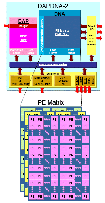
Fig.1 Architecture of DAPDNA-2 Dynamically Reconfigurable Processor
Connected Component Labeling
Connected Component Labeling (CCL) is an important and time-consuming task commonly used in image recognition. By CCL, input image data, from a camera or other source, is processed to extract portions that have a particular meaning. The spatial correlations in binarized input image pixels are searched and a unique ID is labeled to the group of the pixels which are neighboring each other. The connections of the pixels can not be completely resolved until entire input image is scanned, therefore, multiple stages are required to resolve all labels.
Detail of the CCL Algorithm for DNA
The algorithm consists of three stages, First Pass Labeling, Integration, and Final Pass Labeling. Each stage is represented as one DNA Configuration (see Fig.2).
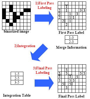
Fig.2 Labeling Flow
In First Pass Labeling, a binarized input image is scanned. Then, at every clock cycle, set of 2x2 pixels, named block, are labeled in a pipeline manner, because 2x2 pixels must be always labeled the same value as long as a pixel exists. The label here is called First Pass Label, some of which may connect with each other in the later part of the image. A block and six neighboring pixels are scanned from the top left to the bottom right of the image (see Fig.3). d(i-1,j-1)d(i+1,j)d(i,j)d(i,j+1)d(i+1,j+1)d(i-1,j)d(i-1,j+1)d(i-1,j+2)d(i,j-1)d(i+1,j-1)a) Input BinarizedImaged(i,j): input binarizeddata (i:row, j:column) l(i-1,j-1)l(i+1,j)l(i,j)l(i,j+1)l(i+1,j+1)l(i-1,j)l(i-1,j+1)l(i-1,j+2)l(i,j-1)l(i+1,j-1)b) Final Pass Labell(i,j): First Pass Label (i:row, j:column)
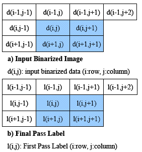
Fig.3 Labeling Window
These 10 pixels are named as window. There are four types of labeling based on the bit pattern of the window: 1) Nop: no labeling occurs, since a block contains all 0s, 2) New: new label value is assigned to the block due to no neighbors, 3) Copy: label value is copied from a neighbor to the block according to their relationship, 4) Merge: in addition to Copy, Merge Information (a pair of labels) is generated from multiple neighboring labels.
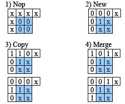
Fig.4 Types of Labeling (Nop, New, Copy, and Merge)
Once First Pass Labeling is done, DNA Configuration is switched to the next stage, Integration. In Integration stage the Integration Table is generated, in which First Pass Labels are translated into Final Pass Labels. FSM (Finite State Machine) is implemented on DNA by means of the microcode in a RAM element. By the FSM, the Merge Information is searched to find the connectivity among First Pass Labels, and all First Pass Labels connecting each other are assigned one unique Final Pass Label.
In Final Pass Labeling, the Integration Table translates First Pass Labels into Final Pass Labels. The characteristics of a group of pixels belonging to IP/SOC 2005 – December 7-8, 2005 2 a particular Final Pass Label, such as the coordinate, area, and box size, are also calculated in parallel.
CCL DNA Implementation
Fig.5 a) depicts a PE structure overview of First Pass Labeling DNA Configuration. Binarized image is loaded from DDR SDRAM to PE Matrix. Then ten bits are cut out by using EXE element (configured as a shift register) to form a window. The bits in the window are used as the address for the LUT where microcodes are stored. The microcodes are defined based on the relationship between the bit pattern in a window and the labeling type (Nop, New, Copy, or Merge). The LUT output forms control signals which select appropriate label, according to the labeling type. Merge Information is also generated based on the control signal.
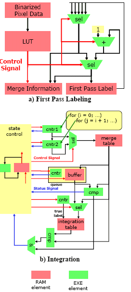
Fig.5 PE Structure Overview
Fig.5 b) describes a PE structure overview of Integration. A FSM is constructed by RAM element FSM mode (yellow box in the left side of the figure). Once Integration DNA Configuration runs, the FSM RAM element asserts the control signals (red line in the figure) and the Integration algorithm is initiated according to the microcodes in the RAM element. Status signals, such as merge table end, queue empty, and label match, are sent back to the FSM RAM element as the part of the FSM RAM address. The status signals and the RAM data outputs compose the address to the FSM RAM element, so that the current status determines the next state, that is, FSM RAM address.
Fig 6 shows the actual PE mapping of First Pass Labeling DNA Configuration. It is described on DNA Designer, the DNA development tool. The figure represents only one segment out of six segments. First Pass Labeling consumes about 60% of total DNA PE resources. Blue boxes represent active PEs while gray boxes are unused PEs.
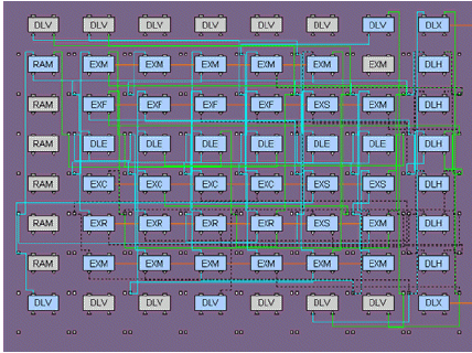
Fig.6 DNA mapping (segment one)
Labeling engine is represented as a C function running on DAP. In labeling engine DNA control libraries are called, so that DNA configuration data load, bank switch, DNA run, and DNA stop are performed by simply call the libraries. Fig.7 describes how DNA is controlled by DAP C code through DNA control library.
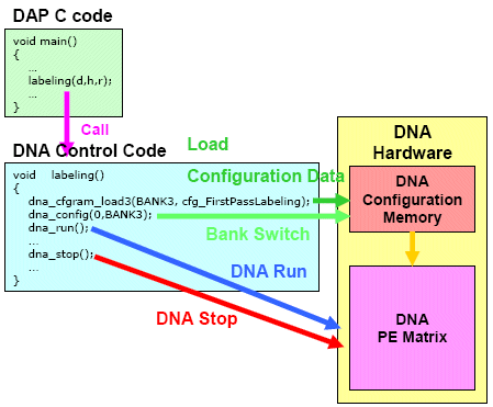
Fig.7 DNA Control Library
Experimental Result
DAPDNA-2 device is fabricated on Fujitsu 0.11um technology and runs at 166MHz. The CCL algorithm above is implemented on DAPDNA-EB5 Evaluation board. Sample image size is 4096x256 pixels. The experimental result is listed in Table.1. As described in the table the results vary depending on the sample image. The processing time for DAPDNA-2 depends on the number of merges as expected. This is because Integration processing time varies according to the number of merges (O(n^2) n: number of merges), while First pass and Final pass processing time are simply depending on the input image size (O(n) n: input image pixels). It is at least over 30 times faster than Pentium4 3.2GHz for the same algorithm.
Table.1 Experimental Resulta) Summary of Sample Input Image
| Number of Blocks Containing Objects | Number of First Pass Label | Number of Merges | Number of Final Pass Label | |
| 1 | 12683 | 194 | 190 | 24 |
| 2 | 24702 | 455 | 484 | 21 |
| 3 | 11617 | 3908 | 1523 | 2702 |
| 4 | 79603 | 11 | 0 | 11 |
b) Processing Time (ms)
| Pentium4 (3.2GHz) | DAPDNA-2 (166MHz) | Performance Raito | |
| 1 | 272.246 | 3.762 | 72.4 |
| 2 | 929.900 | 5.084 | 182.9 |
| 3 | 368.630 | 12.258 | 30.1 |
| 4 | 923.300 | 3.585 | 257.5 |

Fig.8 Sample Input Image
Application Example
In addition to the CCL, other image processing algorithms, such as filtering, shading and pattern matching, can also be implemented on DAPDNA-2 by means of the Dynamic Reconfiguration.
Fig.9 shows an example of a visual inspection system constructed by DAPDNA-2. The green boxes represent DNA Configuration and the blue boxes represent the data to be processed. The input data from the camera is captured by the FPGA, and passed to DAPDNA-2 through Direct I/O interface. Once one frame of the image is stored in DDR SDRAM, DNA starts a process. First, pre-processes, such as shading, average filter and binarization, are performed in the first DNA Configuration. Second, the labeling engine executes the CCL algorithm and generates the characteristic information as the result. Then, the characteristics of each Final Pass Label, representing a defect of a material under the inspection, are analyzed by a pattern matching to define the type of the defect. Finally, the defect information is transferred to a host PC through the PCI interface. Pre-processshading,average,filtering,binarizationPatternMatchingoriginalimage datafilteredimage databinarizedimage dataFinal PassLabelCharacteristicscoordinate,box size, areadefectinformationDirect I/ODAPDNA-2DDR SDRAMPCIcameraFPGADNA loadDNA storeConnectedComponentLabelingPre-storeConnectedComponentLabeling
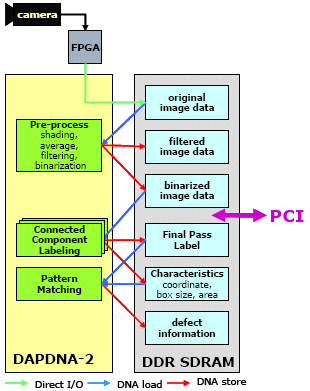
Fig.9 Visual Inspection System Platform
Fig.10 depicts a board block diagram of visual inspection system by DAPDNA2 chips as an example. Each DAPDNA2 chip can be programmed according to the system requirement, therefore, this board can be applied for various product lines. A system with DAPDNA-2 can be a universal hardware platform for visual inspection systems which would save significant amount of time for hardware development.
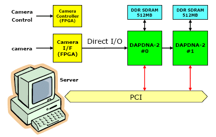
Fig.10 Visual Inspection System Board Block Diagram
Development Tools
IPFlex Inc. provides DAPDNA-FWII, the IDE tool for DAPDNA-2. In addition to the regular IDE functionality, DNA designing tool is included, named DNA Designer. In DNA Designer a developer can design DNA PE matrix easily by a schematic editor like GUI and the design can be simulated and tested immediately. DNA Designer compiles the design to the physical DNA Configuration data in which all PEs are physically placed and routed.
DAPDNA-FWII can perform a whole chip simulation, in which both DAP and DNA are simulated simultaneously. Once a designer is satisfied with the whole chip simulation, then the same binary can be run on a real board.
DFC (Data Flow C) is an alternative way of designing DNA Configuration. DFC is a C like language in which some special notations are added to ANSI C in order to specify the parallelism and timing. Once an algorithm is written in DFC, the Compiler compiles the DFC source code and generates DNA configuration data.
Matlab/Simulink path is also provided. A design described in Simulink can be transferred to a DNA Configuration.
Fig.11 describes the design flow of DAPDNA-2.
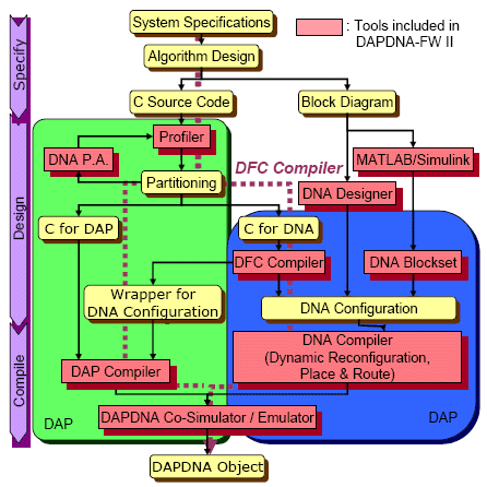
Fig.11 Design Flow
Conclusion
The labeling engine performs the CCL at very high speed by means of the DAPDNA-2 architecture with the optimized algorithm. In addition, various algorithms can be implemented on a single hardware platform on demand. A system with DAPDNA-2 can provide flexibility, high performance, and short development cycle all at once. In the near future Dynamically Reconfigurable Processor will be one of the major hardware platform for the area, in which both high performance and flexibility are required.
References
[1] Tomoyoshi Sato, Kosuke Shiba, Tadashi Matsuoka, Kenji Ikeda, Hiroyuki Watanabe, Mitsuaki Ukiya. "Dynamic Reconfigurable Processor from IPFlex Inc. DAPDNA Dynamic Reconfigurable Processor". IPBased SoC Design 2003, Nov 2003.
[2] Tomoyoshi Sato, "DAPDNA-2: A Dynamically Reconfigurable Processor with 376 32-bit Processing Elements", Hot Chips 17, Aug 2005.
[3] Kuang-Bor Wang, Tsorng-Lin Chia, Zen Chen, Der-Chyuan Lou, "Parallel Execution of a Connected Component Labeling Operation on a Linear Array Architecture". Journal of Information Science and Engineering, Vol.19 No.2, pp. 353-370, Mar 2003.
[4] Eril Mozef, Serge Weber, Jamal Jaber, and Gerard Prieur, "Parallel architecture dedicated to image component labeling in O(n Logn): FPGA implementation". Proc. SPIE, Vol. 2784, pp.120-125, 1996.
Related Semiconductor IP
- UFS 5.0 Host Controller IP
- PDM Receiver/PDM-to-PCM Converter
- Voltage and Temperature Sensor with integrated ADC - GlobalFoundries® 22FDX®
- 8MHz / 40MHz Pierce Oscillator - X-FAB XT018-0.18µm
- UCIe RX Interface
Related Articles
- Interstellar: Fully Partitioned and Efficient Security Monitoring Hardware Near a Processor Core for Protecting Systems against Attacks on Privileged Software
- Physical Design Exploration of a Wire-Friendly Domain-Specific Processor for Angstrom-Era Nodes
- A Direct Memory Access Controller (DMAC) for Irregular Data Transfers on RISC-V Linux Systems
- MultiVic: A Time-Predictable RISC-V Multi-Core Processor Optimized for Neural Network Inference
Latest Articles
- A Scalable Open-Source QEC System with Sub-Microsecond Decoding-Feedback Latency
- SNAP-V: A RISC-V SoC with Configurable Neuromorphic Acceleration for Small-Scale Spiking Neural Networks
- An FPGA Implementation of Displacement Vector Search for Intra Pattern Copy in JPEG XS
- A Persistent-State Dataflow Accelerator for Memory-Bound Linear Attention Decode on FPGA
- VMXDOTP: A RISC-V Vector ISA Extension for Efficient Microscaling (MX) Format Acceleration