An Innovative RF CMOS IP Using a 10 GHz VCO for Direct Conversion WLAN
by Laurent Perraud, Marc Recouly, Christophe Pinatel, Jean-Louis Bonnot, Nicolas Sornin, Frederic Benoist, Olivier Gibrat, Myriam Massei - NewLogic Technologies
1 INTRODUCTION.
If the Wireless LAN market is still growing, Wireless LAN solutions are already in a cost reduction phase. Conceiving WLAN solutions nowadays requires a high-level approach where the final chipset may be better partitioned or reduced to one chip, where the number of external components has to be reduced, where the die size and the technology choice is crucial. The radio chip, for instance, has to be compliant with the numerous standards of the WLAN market, used in at least four radio-frequency bands.
We present here a WLAN radio where the system architecture solves the sum of problems created by multi-band and multi-standard applications. Our solution is compliant with the 802.11a/b/g standards. Then we present some of the techniques used in design to build this solution as a highly integrated, reduced die size, chip in a 0.18um RFCMOS low cost technology. This chip design is available as an Intellectual Property product.
2 RADIO ARCHITECTURE: A DIRECT CONVERSION SYSTEM.
Several publications tried to deal with the choice of the radio architecture for WLAN applications. First solutions in the 5 GHz band were based on heterodyne technique. Reduction of cost through reduced die size and removal of external components pushes to avoid these solutions in the next generation of radios. IF-sampled radio architecture are still too power inefficient for the 20 MHz signal bandwidth to be a serious candidate. The final choice resides in direct conversion architecture against low-IF architecture. The difficulty of this choice is in fact defining the correct set of selection criteria. We present here the set of parameters that made us choose the direct conversion scheme. Fig. 1 shows a high-level block diagram of our radio architecture.
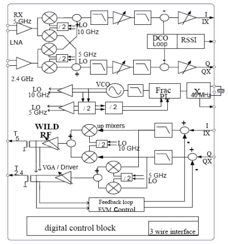
Fig1. Block Diagram of the Radio Architecture
2.1 Multi-band direct conversion receiver with advanced DC offset control and signal detection.
The receive path is the circuit subset where the choice between low-IF and direct conversion system is the most problematic. For handling OFDM signals at high data rates, one of the most important criteria is the DC offset control along the analog baseband chain of gain and filtering.
In the case of OFDM signals whose baseband bandwidth of interest is about 9 MHz, low-IF architecture are using an IF, intermediate frequency, at 10 MHz. This enables the use of on-chip 1 MHz AC-coupling after down mixing. However these systems need twice-higher cut-off frequency analog filters, with extremely high I and Q matching in order to provide good image rejection. To provide a good image rejection it is also preferable to use band-pass complex filter. The main disadvantage of these filters is their power consumption as well as their poor adaptability to different signal bandwidth and different standards. Therefore most system using low-if architecture for OFDM are using a different analog path for CCK modulated signal. This solution is leading then to a system with increased die size and increased power consumption.
Our approach was directly driven by our clear insight in the OFDM signal characteristic. Concentrating our efforts on the DC offset correction for the particular case of the OFDM signals opened the door to the direct conversion receiver and to smaller die size and lower power consumption. DC offset correction systems for direct conversion receiver are usually equivalent to high pass filters. Fig 2 shows an architecture example. However, these systems face the challenge of having a cut-off frequency low enough and a frequency response steep enough so that the modulated signal is not impacted. In the case of the architecture of Fig 1, implementing a low frequency cut-off system implies a very size consuming low-pass filter. The second draw back is the settling time for an impulse response in this system that may become too large (longer than the preamble) in the case of OFDM at high data rates: the correction system must converge before the data of the packet are present. Therefore the DC offset system bandwidth, in the case of OFDM signals, has for upper bound the first carrier starting at 156 kHz and for lower bound the impulse response settling time to be below 2 us i.e. 500 kHz. The mission seemed impossible. However a thorough analysis of the preamble in the OFDM signal showed that none of the first 4 carriers where used. There was more than 1 MHz bandwidth available for the DC correction system during at least the preamble time (8 us) ! The DC offset correction system architecture came from this statement: fast converging system with a DC offset held during the rest of the packet reception. The mixed-signal design implementation that we used was particularly adapted to answer this problem. This DC offset correction system proved to be just as efficient for other standards.
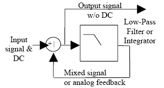
Fig 2. Classic DC Offset Correction
The RF Low Noise Amplifier for the 5 GHz band was designed to have a constant gain and a constant noise figure over 1 GHz RF input bandwidth. This can only be achieved by a self-calibrating frequency tuning system. A differential structure has been chosen to limit the effect of power supply and ground bondings on the LNA gain and input matching.
2.2 Multi-band cartesian feedback transmitter.
The choice of direct conversion system for the transmitter resides in the achievable RF power dynamic range. As a matter of fact, the dynamic range required by the standards cannot rely only on the analog baseband transmit strip because the inherent LO leakage power caused by mixers does not depend on the analog baseband level. Therefore the RF preamplifier after the mixer needs to accommodate a high dynamic range so that the level of the signal and the LO leakage stay proportional. The other challenge was the maximum power to deliver. 5 GHz actual PA needs at least 0 dBm average power to deliver 5 dBm. Taking into account the crest factor of the OFDM modulation at high data rates, the on-chip preamplifier needs to deliver 10 dBm peak.
This even extends the dynamic range by its upper bound. Heterodyne systems allow to split the dynamic range into two stages at two different frequencies with a better inherent isolation between those stages. However with direct conversion transmitters, the implementation of a cartesian feedback is easier especially because there is only one RF frequency to deal with. Fig 3 shows the block diagram of the transmitter with its cartesian feedback. The benefit of this architecture is the tremendous improvement for linearity at higher power, at similar power efficiency, compared to any other type of architecture. The main issue with whole transmit frequency band. Designing this cartesian feedback for applications from 4.9 GHz up to 5.9 GHz , where the phase rotation in the transmit RF path before the feedback can reach values up to 540 degrees, required another patented innovation. The block diagram of Fig 3. includes a phase rotator, i.e. a baseband analog block that performs on the down-converted signals a complex multiplication by exp(j*theta) where theta is the required phase for optimal loop stability. Theta has an optimum value for each transmit RF frequency that can be determined by a patented calibration algorithm.
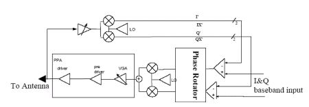
Fig 3. Architecture of the Cartesian Feedback Direct Conversion Transmitter
This system has been implemented for the transmitter 5 GHz as well as for the 2.4 GHz transmitter. The preamplifiers also provides a single-ended, 50 Ohms impedance matched, output suitable for power amplifiers with on-chip transformer and without any external components. An Error Vector Magnitude (EVM) of 4% at 0 dBm average power has been measured in the 5 GHz band and in the 2.4 GHz band.
2.3 12 GHz fractional-N synthesizer.
The radio architecture of both the receiver and the transmitter has been conceived as direct conversion systems. The RF synthesizer had to generate 2.4 GHz as well as 4.9 GHz to 5.9 GHz in phase and in-quadrature signals. We used a standard RF topology for LO generation, working with a single LO at double the frequency for the 5 GHz range and at four times the frequency for the 2.4 GHz range. This is the simplest architecture to avoid pulling at the transmit frequency. However the pulling at twice the transmit frequency exits. Many candidate architectures for WLAN at 5 GHz have been presented with LO at fractional portion of the transmit or receive frequency. This avoids the second harmonic pulling but complexifies the design and leads to increased die size and power consumption. Here again, in the case of OFDM at 5 GHz a closer look at the frequency spectrum of the transmitted signals led us to carefully choose the bandwidth of the PLL-synthesizer loop so that the first carrier at 312.5 kHz from the carrier would not have any significant power inside the PLL bandwidth loop.
The choice of building a fractional-N synthesizer was made by the fact that the different standards requires 1 MHz step at 5 GHz. Building an integer PLL at 1 MHz would have led to a PLL loop bandwidth lower than 50 kHz, with a locking time that would have too long to support the frequency agility option of WLAN standards. Moreover pulling immunity and frequency step response of the loop would suffer from this low PLL bandwidth. Low bandwidth PLL are also harder to fully integrate due to the size of their loop filter. Another drawback of the integer PLL is the high division ratio in the loop (10 GHz over 1 MHz) that would make the residual integrated phase noise required by the OFDM standards almost unreachable. Therefore our choice has been to implement a 40 Mhz fractional-N PLL with the possibility to synthesize frequencies with steps down to 4 kHz.
The VCO was then specified to be able to run from 9.6 GHz (2.4 GHz x 4) to 11.77 GHz (5.885 GHz x 2). This design could be achieved using only one VCO by creating and characterizing a full custom varactor device that allows, used inside a digitally controlled array, over 2 GHz range with an analog control having only 100 MHz/V frequency tuning slope. The high frequency operation enabled us to use high-Q (25) on-chip inductor. The varactor array combined with such a high-Q on-chip inductor creates a resonance tank with a peak Q of 18 at 12 GHz. To reach varactor regions where the VCO frequency would be less sensitive to supply voltage an innovative 3 V charge pump operating with an external supply voltage of 1.8 V has been built without using thick oxide devices and while still protecting internal devices from higher voltage than the technology allows.
As a result a fully integrated (no-external components) 12 GHz synthesizer has been built with a residual RMS jitter at 6 GHz of only 400 fs.
3 RF CMOS DESIGN ISSUES UP TO 12 GHZ.
3.1 RF CMOS design specificity
3.1.1 Transistor cut-off frequency and isolation problems in CMOS.
The CMOS 0.18um devices used to design have a transition frequency (Ft) of 40 GHz (10 GHz) for the NMOS (PMOS respectively). Most standard blocks architecture using complementary operation of the PMOS and NMOS were not usable in the 5 GHz path, especially when stringent production corners in process variations and temperature operating range must be satisfied. Fallback plans are not numerous. Power hungry structures with ECL NMOS & resistance were used only when the LC resonance where not usable. Realizing multi-stage amplification with all stages built on an LC resonance is very problematic in CMOS due the poor inter-stage isolation caused by the high gate-drain capacitance. Resonance frequencies of early stages depend of the miller-effect effective capacitance of the next stage and therefore depend of the effective gain of the next stage. This poor isolation can create inter-stages pulling effect and AM/PM distortion in all the RF paths including L-Cgate resonance.
3.1.2 Low voltage operation.
All radio blocks, although the specification required operation at a minimum power supply of 1.8 V, have been measured functional with a 1.5 V power supply. CMOS design can accommodate very low supply voltage. However, the power supply limits the transmit paths maximum output swing and therefore output power. RF on-chip combiner can be used but their efficiency only allows a small ratio between the output voltage swing and the power supply. Current amplifications in RF and baseband might require more stages at lower power supply. Each stage has on overhead current consumption that tend to increase the total average current consumption.
In order to take advantage of the low power supply in the case of battery powered mobile devices, where the usual power supply is around 3.6 V, the chip must tolerate a DC-DC step-down converter associated with a voltage regulator on its power supply. This forces more stringent specifications on all power supply sensitivity parameters. The price of these components must also be included in the bill of material.
3.1.3 Transistor noise and flicker noise issues.
One of the drawbacks of advanced CMOS technologies compared to bipolar technologies is the higher corner of flicker noise. There are only some very specific blocks where the flicker noise can become a roadblock. However, new wireless standards use larger bandwidth modulations where signal content near the carrier (or near DC in analog baseband) is not impacted by the transceiver noise. The use of CMOS is therefore not a penalty for these systems for noise considerations.
Moreover, measurement shows that white noise such as shot noise is lower in current CMOS technology than with their BiCMOS competitors. NFmin for the LNA have been measured below 1 dB at 5 GHz. Even if the input matching for the LNA might be more problematic, this is a serious advantage to build a receive chain with a NF of 4.5 dB from chip input to analog baseband output.
3.2 Low power consumption: system level optimization.
Current consumption sizing has been described earlier at the design and RF architecture level. Another type of optimization can be conducted at the application system level. Looking into the standards, we were able to categorize idle times into many different idle modes, characterized mainly by their wake-up time. When the hosted software decides to put the baseband and the radio in sleep mode, the waking up time may be different than when just the radio is put in a sleep mode. Baseband processors are now implementing a functionality with early packet error detection where the radio in receive mode is put in a sleep mode as soon as we can be sure that the received packet will be discarded. This type of optimization can ensure savings up to 20 % in overall power consumption of the system. For this reason up to 5 different idle modes have been implemented in the radio, with power consumption down to 5 uA and waking up time ranging from 2 us to 5 ms.
3.3 Die size, chip cost and yield control in RF CMOS.
Our multi-band, multi-standard radio IP has a core die size of 9.6 mm2. This success due to close interaction between RF system engineers and RF designers has a serious cost advantage knowing that the technology process used is a standard 0.18 um CMOS process with the triple-well option, the MIM capacitor option and the thick top metal option. Recurrent cost concerns seem to be raised about yield in the fabrication line of RF CMOS circuits. Most concerns come from either matching problems or process parameters controls. CMOS is more dependent on lithography than vertical bipolar devices. As our measurements are only starting we can provide limited dispersion numbers. But the few parameters that we have are very encouraging for future yields. We measured around 70mV of standard deviation on the natural output offset of the analog baseband strip with 27 dB of gain. This numbers is at least 4 times lower than the DC offset correction range. Another parameter measured was the central frequency of the VCO (dependent in our design of several process parameters) with a standard deviation was 0.4%.
4 CONCLUSION
We presented a radio Intellectual Property core compliant with the 802.11a/b/g standards. This core has been implemented using a direct conversion architecture that would optimize die size and power consumption. We have been able to answer the challenge of designing a manufacturable product in a 0.18 um RF CMOS technology with internal frequencies up to 12 GHz. Our next challenge is mainly the integration of the RF core with some digital baseband functionality.
ACKNOWLEDGMENT
The authors would like to thank Jean-Marc Glasser for his work during the initial phase of the development, Olivier Fargant for its help during measurements, Alexandra Troubat, Patrice Gattel and Franck Pourchet for the physical design. Our company would like to thank TSMC for their support during our RF developments.
1 INTRODUCTION.
If the Wireless LAN market is still growing, Wireless LAN solutions are already in a cost reduction phase. Conceiving WLAN solutions nowadays requires a high-level approach where the final chipset may be better partitioned or reduced to one chip, where the number of external components has to be reduced, where the die size and the technology choice is crucial. The radio chip, for instance, has to be compliant with the numerous standards of the WLAN market, used in at least four radio-frequency bands.
We present here a WLAN radio where the system architecture solves the sum of problems created by multi-band and multi-standard applications. Our solution is compliant with the 802.11a/b/g standards. Then we present some of the techniques used in design to build this solution as a highly integrated, reduced die size, chip in a 0.18um RFCMOS low cost technology. This chip design is available as an Intellectual Property product.
2 RADIO ARCHITECTURE: A DIRECT CONVERSION SYSTEM.
Several publications tried to deal with the choice of the radio architecture for WLAN applications. First solutions in the 5 GHz band were based on heterodyne technique. Reduction of cost through reduced die size and removal of external components pushes to avoid these solutions in the next generation of radios. IF-sampled radio architecture are still too power inefficient for the 20 MHz signal bandwidth to be a serious candidate. The final choice resides in direct conversion architecture against low-IF architecture. The difficulty of this choice is in fact defining the correct set of selection criteria. We present here the set of parameters that made us choose the direct conversion scheme. Fig. 1 shows a high-level block diagram of our radio architecture.

Fig1. Block Diagram of the Radio Architecture
2.1 Multi-band direct conversion receiver with advanced DC offset control and signal detection.
The receive path is the circuit subset where the choice between low-IF and direct conversion system is the most problematic. For handling OFDM signals at high data rates, one of the most important criteria is the DC offset control along the analog baseband chain of gain and filtering.
In the case of OFDM signals whose baseband bandwidth of interest is about 9 MHz, low-IF architecture are using an IF, intermediate frequency, at 10 MHz. This enables the use of on-chip 1 MHz AC-coupling after down mixing. However these systems need twice-higher cut-off frequency analog filters, with extremely high I and Q matching in order to provide good image rejection. To provide a good image rejection it is also preferable to use band-pass complex filter. The main disadvantage of these filters is their power consumption as well as their poor adaptability to different signal bandwidth and different standards. Therefore most system using low-if architecture for OFDM are using a different analog path for CCK modulated signal. This solution is leading then to a system with increased die size and increased power consumption.
Our approach was directly driven by our clear insight in the OFDM signal characteristic. Concentrating our efforts on the DC offset correction for the particular case of the OFDM signals opened the door to the direct conversion receiver and to smaller die size and lower power consumption. DC offset correction systems for direct conversion receiver are usually equivalent to high pass filters. Fig 2 shows an architecture example. However, these systems face the challenge of having a cut-off frequency low enough and a frequency response steep enough so that the modulated signal is not impacted. In the case of the architecture of Fig 1, implementing a low frequency cut-off system implies a very size consuming low-pass filter. The second draw back is the settling time for an impulse response in this system that may become too large (longer than the preamble) in the case of OFDM at high data rates: the correction system must converge before the data of the packet are present. Therefore the DC offset system bandwidth, in the case of OFDM signals, has for upper bound the first carrier starting at 156 kHz and for lower bound the impulse response settling time to be below 2 us i.e. 500 kHz. The mission seemed impossible. However a thorough analysis of the preamble in the OFDM signal showed that none of the first 4 carriers where used. There was more than 1 MHz bandwidth available for the DC correction system during at least the preamble time (8 us) ! The DC offset correction system architecture came from this statement: fast converging system with a DC offset held during the rest of the packet reception. The mixed-signal design implementation that we used was particularly adapted to answer this problem. This DC offset correction system proved to be just as efficient for other standards.

Fig 2. Classic DC Offset Correction
The RF Low Noise Amplifier for the 5 GHz band was designed to have a constant gain and a constant noise figure over 1 GHz RF input bandwidth. This can only be achieved by a self-calibrating frequency tuning system. A differential structure has been chosen to limit the effect of power supply and ground bondings on the LNA gain and input matching.
2.2 Multi-band cartesian feedback transmitter.
The choice of direct conversion system for the transmitter resides in the achievable RF power dynamic range. As a matter of fact, the dynamic range required by the standards cannot rely only on the analog baseband transmit strip because the inherent LO leakage power caused by mixers does not depend on the analog baseband level. Therefore the RF preamplifier after the mixer needs to accommodate a high dynamic range so that the level of the signal and the LO leakage stay proportional. The other challenge was the maximum power to deliver. 5 GHz actual PA needs at least 0 dBm average power to deliver 5 dBm. Taking into account the crest factor of the OFDM modulation at high data rates, the on-chip preamplifier needs to deliver 10 dBm peak.
This even extends the dynamic range by its upper bound. Heterodyne systems allow to split the dynamic range into two stages at two different frequencies with a better inherent isolation between those stages. However with direct conversion transmitters, the implementation of a cartesian feedback is easier especially because there is only one RF frequency to deal with. Fig 3 shows the block diagram of the transmitter with its cartesian feedback. The benefit of this architecture is the tremendous improvement for linearity at higher power, at similar power efficiency, compared to any other type of architecture. The main issue with whole transmit frequency band. Designing this cartesian feedback for applications from 4.9 GHz up to 5.9 GHz , where the phase rotation in the transmit RF path before the feedback can reach values up to 540 degrees, required another patented innovation. The block diagram of Fig 3. includes a phase rotator, i.e. a baseband analog block that performs on the down-converted signals a complex multiplication by exp(j*theta) where theta is the required phase for optimal loop stability. Theta has an optimum value for each transmit RF frequency that can be determined by a patented calibration algorithm.

Fig 3. Architecture of the Cartesian Feedback Direct Conversion Transmitter
This system has been implemented for the transmitter 5 GHz as well as for the 2.4 GHz transmitter. The preamplifiers also provides a single-ended, 50 Ohms impedance matched, output suitable for power amplifiers with on-chip transformer and without any external components. An Error Vector Magnitude (EVM) of 4% at 0 dBm average power has been measured in the 5 GHz band and in the 2.4 GHz band.
2.3 12 GHz fractional-N synthesizer.
The radio architecture of both the receiver and the transmitter has been conceived as direct conversion systems. The RF synthesizer had to generate 2.4 GHz as well as 4.9 GHz to 5.9 GHz in phase and in-quadrature signals. We used a standard RF topology for LO generation, working with a single LO at double the frequency for the 5 GHz range and at four times the frequency for the 2.4 GHz range. This is the simplest architecture to avoid pulling at the transmit frequency. However the pulling at twice the transmit frequency exits. Many candidate architectures for WLAN at 5 GHz have been presented with LO at fractional portion of the transmit or receive frequency. This avoids the second harmonic pulling but complexifies the design and leads to increased die size and power consumption. Here again, in the case of OFDM at 5 GHz a closer look at the frequency spectrum of the transmitted signals led us to carefully choose the bandwidth of the PLL-synthesizer loop so that the first carrier at 312.5 kHz from the carrier would not have any significant power inside the PLL bandwidth loop.
The choice of building a fractional-N synthesizer was made by the fact that the different standards requires 1 MHz step at 5 GHz. Building an integer PLL at 1 MHz would have led to a PLL loop bandwidth lower than 50 kHz, with a locking time that would have too long to support the frequency agility option of WLAN standards. Moreover pulling immunity and frequency step response of the loop would suffer from this low PLL bandwidth. Low bandwidth PLL are also harder to fully integrate due to the size of their loop filter. Another drawback of the integer PLL is the high division ratio in the loop (10 GHz over 1 MHz) that would make the residual integrated phase noise required by the OFDM standards almost unreachable. Therefore our choice has been to implement a 40 Mhz fractional-N PLL with the possibility to synthesize frequencies with steps down to 4 kHz.
The VCO was then specified to be able to run from 9.6 GHz (2.4 GHz x 4) to 11.77 GHz (5.885 GHz x 2). This design could be achieved using only one VCO by creating and characterizing a full custom varactor device that allows, used inside a digitally controlled array, over 2 GHz range with an analog control having only 100 MHz/V frequency tuning slope. The high frequency operation enabled us to use high-Q (25) on-chip inductor. The varactor array combined with such a high-Q on-chip inductor creates a resonance tank with a peak Q of 18 at 12 GHz. To reach varactor regions where the VCO frequency would be less sensitive to supply voltage an innovative 3 V charge pump operating with an external supply voltage of 1.8 V has been built without using thick oxide devices and while still protecting internal devices from higher voltage than the technology allows.
As a result a fully integrated (no-external components) 12 GHz synthesizer has been built with a residual RMS jitter at 6 GHz of only 400 fs.
3 RF CMOS DESIGN ISSUES UP TO 12 GHZ.
3.1 RF CMOS design specificity
3.1.1 Transistor cut-off frequency and isolation problems in CMOS.
The CMOS 0.18um devices used to design have a transition frequency (Ft) of 40 GHz (10 GHz) for the NMOS (PMOS respectively). Most standard blocks architecture using complementary operation of the PMOS and NMOS were not usable in the 5 GHz path, especially when stringent production corners in process variations and temperature operating range must be satisfied. Fallback plans are not numerous. Power hungry structures with ECL NMOS & resistance were used only when the LC resonance where not usable. Realizing multi-stage amplification with all stages built on an LC resonance is very problematic in CMOS due the poor inter-stage isolation caused by the high gate-drain capacitance. Resonance frequencies of early stages depend of the miller-effect effective capacitance of the next stage and therefore depend of the effective gain of the next stage. This poor isolation can create inter-stages pulling effect and AM/PM distortion in all the RF paths including L-Cgate resonance.
3.1.2 Low voltage operation.
All radio blocks, although the specification required operation at a minimum power supply of 1.8 V, have been measured functional with a 1.5 V power supply. CMOS design can accommodate very low supply voltage. However, the power supply limits the transmit paths maximum output swing and therefore output power. RF on-chip combiner can be used but their efficiency only allows a small ratio between the output voltage swing and the power supply. Current amplifications in RF and baseband might require more stages at lower power supply. Each stage has on overhead current consumption that tend to increase the total average current consumption.
In order to take advantage of the low power supply in the case of battery powered mobile devices, where the usual power supply is around 3.6 V, the chip must tolerate a DC-DC step-down converter associated with a voltage regulator on its power supply. This forces more stringent specifications on all power supply sensitivity parameters. The price of these components must also be included in the bill of material.
3.1.3 Transistor noise and flicker noise issues.
One of the drawbacks of advanced CMOS technologies compared to bipolar technologies is the higher corner of flicker noise. There are only some very specific blocks where the flicker noise can become a roadblock. However, new wireless standards use larger bandwidth modulations where signal content near the carrier (or near DC in analog baseband) is not impacted by the transceiver noise. The use of CMOS is therefore not a penalty for these systems for noise considerations.
Moreover, measurement shows that white noise such as shot noise is lower in current CMOS technology than with their BiCMOS competitors. NFmin for the LNA have been measured below 1 dB at 5 GHz. Even if the input matching for the LNA might be more problematic, this is a serious advantage to build a receive chain with a NF of 4.5 dB from chip input to analog baseband output.
3.2 Low power consumption: system level optimization.
Current consumption sizing has been described earlier at the design and RF architecture level. Another type of optimization can be conducted at the application system level. Looking into the standards, we were able to categorize idle times into many different idle modes, characterized mainly by their wake-up time. When the hosted software decides to put the baseband and the radio in sleep mode, the waking up time may be different than when just the radio is put in a sleep mode. Baseband processors are now implementing a functionality with early packet error detection where the radio in receive mode is put in a sleep mode as soon as we can be sure that the received packet will be discarded. This type of optimization can ensure savings up to 20 % in overall power consumption of the system. For this reason up to 5 different idle modes have been implemented in the radio, with power consumption down to 5 uA and waking up time ranging from 2 us to 5 ms.
3.3 Die size, chip cost and yield control in RF CMOS.
Our multi-band, multi-standard radio IP has a core die size of 9.6 mm2. This success due to close interaction between RF system engineers and RF designers has a serious cost advantage knowing that the technology process used is a standard 0.18 um CMOS process with the triple-well option, the MIM capacitor option and the thick top metal option. Recurrent cost concerns seem to be raised about yield in the fabrication line of RF CMOS circuits. Most concerns come from either matching problems or process parameters controls. CMOS is more dependent on lithography than vertical bipolar devices. As our measurements are only starting we can provide limited dispersion numbers. But the few parameters that we have are very encouraging for future yields. We measured around 70mV of standard deviation on the natural output offset of the analog baseband strip with 27 dB of gain. This numbers is at least 4 times lower than the DC offset correction range. Another parameter measured was the central frequency of the VCO (dependent in our design of several process parameters) with a standard deviation was 0.4%.
4 CONCLUSION
We presented a radio Intellectual Property core compliant with the 802.11a/b/g standards. This core has been implemented using a direct conversion architecture that would optimize die size and power consumption. We have been able to answer the challenge of designing a manufacturable product in a 0.18 um RF CMOS technology with internal frequencies up to 12 GHz. Our next challenge is mainly the integration of the RF core with some digital baseband functionality.
ACKNOWLEDGMENT
The authors would like to thank Jean-Marc Glasser for his work during the initial phase of the development, Olivier Fargant for its help during measurements, Alexandra Troubat, Patrice Gattel and Franck Pourchet for the physical design. Our company would like to thank TSMC for their support during our RF developments.
Related Semiconductor IP
- ReRAM NVM in DB HiTek 130nm BCD
- UFS 5.0 Host Controller IP
- PDM Receiver/PDM-to-PCM Converter
- Voltage and Temperature Sensor with integrated ADC - GlobalFoundries® 22FDX®
- 8MHz / 40MHz Pierce Oscillator - X-FAB XT018-0.18µm
Related Articles
- An Introduction to Direct RF Sampling in a World Evolving Towards Chiplets - Part 1
- CMOS RF SoC design shoots for 60 GHz
- CAST Provides a Functional Safety RISC-V Processor IP for Microchip FPGAs
- SV-LLM: An Agentic Approach for SoC Security Verification using Large Language Models
Latest Articles
- An FPGA-Based SoC Architecture with a RISC-V Controller for Energy-Efficient Temporal-Coding Spiking Neural Networks
- Enabling RISC-V Vector Code Generation in MLIR through Custom xDSL Lowerings
- A Scalable Open-Source QEC System with Sub-Microsecond Decoding-Feedback Latency
- SNAP-V: A RISC-V SoC with Configurable Neuromorphic Acceleration for Small-Scale Spiking Neural Networks
- An FPGA Implementation of Displacement Vector Search for Intra Pattern Copy in JPEG XS