Micro FPGAs and embedded FPGAs
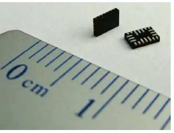
When people hear “FPGA” they think “big, expensive, power hungry”. But it doesn’t need to be that way.
Renesas has announced their Forge FPGA family. Details at their website and in one of the many articles that covered their press release (links below):
https://www.renesas.com/tw/en/products/programmable-mixed-signal-asic-ipproducts/ forgefpga-low-density-fpgas
https://www.eejournal.com/article/renesas-announces-fabulous-forgefpga-family/
Forge FPGAs show that FPGAs don’t have to be big, power hungry and expensive.
Forge FPGAs are tiny, draw standby current measured in micro-amps and as of the press announcement were expected to sell in volume at prices less than 50 cents!

It’s interesting to see how Renesas uses eFPGA to build their product. If you design volume systems you may want to check this out. If you design SoCs, you can get some ideas for how to use small amounts in eFPGA in your SoC.
Forge FPGAs come with a complete tool kit and programming environment: they can be programmed in Verilog or using Renesas’ graphical user interface (IP Block Wizard) where a logic block diagram can be implemented without any Verilog coding; they include a simulator.
Their ForgeFPGA Workshop User Guide is available online:
https://www.renesas.com/us/en/document/gde/forgefpga-workshop-user-guide
The screen shots shown below are Copyright Renesas.
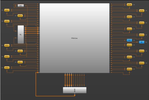
Here is the top level view of the ForgeFPGA in their GUI:

The FPGA core is an EFLX eFPGA tile/array which connects directly to GPIOs, BRAM, PLL, etc.
The user generates the code that runs on the FPGA.
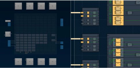
Below is a screen short of P&R results:

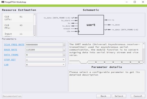
Finally below is an example of an IP Block in their GUI:

EFLX 1K eFPGA Tile for SoC Designs
Renesas shows us that FPGA doesn’t need to be huge and power hungry.
Renesas uses the EFLX® 1K eFPGA Tile in the Forge FPGA and so can you in your SoC to perform “glue logic” functions for GPIO or in parts of your SoC where you need to be able to adapt to unforeseeable changes in customer requirements, protocols or algorithms. Or post-silicon bug fixing.
Currently the EFLX 1K tile is available and silicon proven in TSMC 40ULP. A single tile takes about 1.5 mm2. In TSMC N7 it would only take about 0.2 mm2. With such a small eFPGA you can sprinkle them around your SoC like you do with small ARM cores. Of course, you can also use our EFLX4K in more advanced nodes which is <1 mm2 and available now on 16, 12 and 7nm.
An EFLX 1K tile is a stand alone FPGA with 368 inputs and 368 outputs, each with any optional flip flop, which can connect to your processor or peripheral buses; can control local GPIO with different protocols; or can be a state machine for controlling data paths.
A single EFLX 1K can be programmed as a 16450 UART or a I2C Master or a SPI master.
An EFLX 1K tile can also be arrayed for 2K, 4K, 8K, 16K, or more LUTs. A 16K array would have 4 times the inputs and 4 times the outputs of a single EFLX 1K.
We can port the EFLX 1K tile to any process node with a customer commitment: it takes ~6 months from signed contract and availability of resources and foundry PDK/standard cells.
Please contact us at info@flex-logix.com if you would like to talk to our Solutions Architects to learn more and see how we can assist you solve your problems.
Related Semiconductor IP
- eFPGA on GlobalFoundries GF12LP
- eFPGA IP — Flexible Reconfigurable Logic Acceleration Core
- Heterogeneous eFPGA architecture with LUTs, DSPs, and BRAMs on GlobalFoundries GF12LP
- eFPGA Soft IP
- Radiation-Hardened eFPGA
Related Blogs
- Neural Network Efficiency with Embedded FPGA's
- Addressing Challenges with FPGAs in Space Using the GR716B Microcontroller
- Xilinx ARMs FPGAs, Altera to MIPSify Them
- Why Is Intel Fabbing Achronix FPGAs?
Latest Blogs
- Area, Pipelining, Integration: A Comparison of SHA-2 and SHA-3 for embedded Systems.
- Why Your Next Smartphone Needs Micro-Cooling
- Teaching AI Agents to Speak Hardware
- SOCAMM: Modernizing Data Center Memory with LPDDR6/5X
- Bridging the Gap: Why eFPGA Integration is a Managed Reality, Not a Schedule Risk
