High Bandwidth Memory Evolution from First Generation HBM to the Latest HBM4
HBM4 is the latest generation of the High Bandwidth Memory (HBM) that has become analogous to the Artificial Intelligence (AI) boom that is everywhere in today’s world. HBM is also increasingly being used in other applications like Data centers, autonomous driving systems, servers, cloud computing just to mention few domains where bandwidth and performance in a key requirement.
HBM History
HBM started as an answer to the requirement of higher-width GDDR memory devices which can help with the higher bandwidth and performance needs while keeping the core device architecture still a DRAM with deterministic latency for Read/Write accesses. This new family of DRAMs was designed to work closely with GPU that are used for graphics and other compute intensive tasks. First HBM device standard JESD235 was published by JEDEC in October 2013.
HBM4
HBM4 is the latest generation of device standard for HBM devices. HBM4 devices have improved on several major features as compared to the previous generation of HBM devices. Some of the important changes are listed below:
I/O and DRAM Core Voltage
HBM4 core DRAM voltage has been reduced to 1.05V, with I/O voltage left to vendors to decide. This is a significant improvement over the 1.1V needed for both the DRAM core and I/O for previous generation HBM3 devices. This helps with better power efficiency for HBM4 devices.
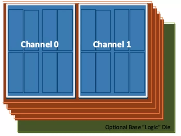
Channels
HBM4 supports upto 32 channels, which is double the number of channels that was possible with HBM3. This is important performance improvement as the number of core per CPU/GPU has gone up.
Directed Refresh Management (DRFM)
HBM4 devices enhance the DRAM capabilities to keep track of the potential data integrity issues by tracking row addresses, which can then be used by the host to send directed refresh management commands thus avoiding potential loss of data arising out of row hammering or other similar attacks. DRFM provides additional flexibility to host and can be used independently of the traditional Refresh Management (RFM) and Adaptive Refresh Management (ARFM) which was also supported by HBM3.
WSO Remapping
Traditionally, HBM devices support the repairs of the broken address and data bus lanes by providing a redundant lane, which can be used to remap via both soft or hard lane repair operations. This has been used to improve the assembly yield. HBM4 devices support a new type of option to do WSO remapping that does not operate on an individual channel. This feature allows for post packaging repair of any potential issues with WSO bus lanes themselves with two additional redundant lanes for the whole IEEE1500 interface.
Decision Feedback Equalizer (DFE)
HBM4 supports the decision feedback equalizer. However, it’s left up to vendors to define the step sizes used for each DFE taps.
Mode Registers
As the number of DRAM features increases, HBM4 devices support MR0-MR19, which are four more than what HBM3 had. These additional mode registers are used for features like DFE, DRFM, etc.
The below table summarizes the various aspects of HBM devices across generations:
|
HBM/HBM2/HBM2E |
HBM3/HBM3E |
HBM4 |
|
|
Burst length |
2 or 4 |
8 |
8 |
|
Prefetch |
256 bits |
256 bits |
256 bits |
|
Banks |
Upto 48 |
Upto 64 |
Upto 64 |
|
Speed (Vendors may support higher/different speed bins) |
3.6 Gbps/pin |
8 Gbps/pin |
8 Gbps/pin |
|
DRAM core voltage |
1.1V |
1.1V |
1.05V |
|
Density per channel |
16Gb |
32Gb |
16Gb |
|
Number of channels |
8 |
16 |
32 |
|
Pseudo channel supported |
HBM: No HBM2: Yes |
Yes |
Yes |
Cadence VIPs offers a comprehensive memory subsystem solution that includes memory models for all generations of High Bandwidth Memory devices (with HBM4 being the latest) compliant to JEDEC specification defined for each of those devices, DFI memory controller/PHY VIPs, and a System Performance Analyzer (SPA) for HBM devices.
If you have any queries, feel free to contact us at talk_to_vip_expert@cadence.com
More information on Cadence HBM4 VIP is available at Cadence VIP memory models website.
Related Semiconductor IP
- HBM4E PHY and controller
- HBM4 PHY IP
- HBM4 Controller IP
- TSMC CLN3FFP HBM4 PHY
- HBM4 Memory Controller
Related Blogs
- High Bandwidth Memory (HBM) at the AI Crossroads: Customization or Standardization?
- HBM3: Next generation memory standard for solving high density and complex computational problems
- The Road to Innovation with Synopsys 224G PHY IP From Silicon to Scale: Synopsys 224G PHY Enables Next Gen Scaling Networks
- Evolution of AMBA AXI Protocol: An Introduction to the Issue L Update
Latest Blogs
- Area, Pipelining, Integration: A Comparison of SHA-2 and SHA-3 for embedded Systems.
- Why Your Next Smartphone Needs Micro-Cooling
- Teaching AI Agents to Speak Hardware
- SOCAMM: Modernizing Data Center Memory with LPDDR6/5X
- Bridging the Gap: Why eFPGA Integration is a Managed Reality, Not a Schedule Risk