The Integrated Design Challenge: Developing Chip, Software, and System in Unison
“We are in an era of pervasive intelligence,” said Shankar Krishnamoorthy, chief product development officer at Synopsys.
Moderating a panel discussion at the inaugural Synopsys Executive Forum, he described the transformative impact of artificial intelligence (AI) and the challenges ahead.
“The dramatic growth in complexity coupled with an accelerated pace of innovation is causing all of us to look hard at our engineering workflows and how to re-engineer them,” Krishnamoorthy said, “from system design and architecture to silicon and software development.”
The industry now faces an integrated design challenge, he noted, where chip, software, and system development must evolve in unison. As AI embeds itself deeper into every compute domain, engineering teams are rethinking how they build and deploy products, re-engineering almost every phase of the design lifecycle — from silicon to systems.
“We’ve evolved from software being primarily written by humans and run on a CPU to a world where software will increasingly be written with machine learning and run on an accelerator,” said Marc Hamilton, vice president of solutions architecture and engineering at NVIDIA. “That fundamental shift — driven by AI — has changed the design of computing.”
Software-defined everything
With the industry’s rapid advances, companies are no longer able to design hardware in isolation. And this is a key reason why software-defined systems now underpin much of AI hardware development.
“You can’t wait for new hardware,” said Hamilton. “The models change so quickly, the hardware needs to be software-defined, and the easiest way is to have a general-purpose processor.”
To support the supersonic evolution of AI, hardware design increasingly centers around modularity and reusability. Instead of waiting a full year or more to bring a chip to market, companies are trying to spin derivatives in months using chiplet architectures and firmware customization.
“The [AI] models are changing a lot faster than the hardware can change,” said Frank Ostojic, SVP and GM of ASIC products at Broadcom. “The ability to have IP that can change quickly with firmware becomes essential.”
This new reality requires new levels of team collaboration.
“It’s coming to a point where hardware/software co-design is absolutely necessary,” said Kevork Kechichian, EVP of solutions engineering at Arm.
At Meta, it’s a similar story. Custom silicon designs for AI workloads rely on cross-team visibility and real workload integration. Through close collaboration with production engineering and software developers, Meta’s silicon teams can anticipate deployment challenges and embed telemetry features early. This tight loop also reduces costs while enhancing agility, enabling Meta to incorporate last-minute features for changing models.
“We take a holistic approach,” said Olivia Wu, AI/ML silicon design lead at Meta. “This enables us to improve software developer efficiency and optimize performance for the actual workload.”
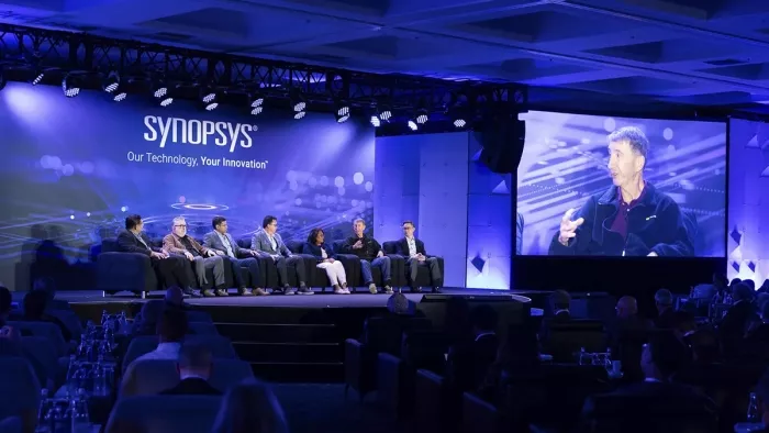
Left to right: Shankar Krishnamoorthy (Synopsys), Kevork Kechichian (Arm), Jitendra Mohan (Astera Labs), Frank Ostojic (Broadcom), Olivia Wu (Meta), Marc Hamilton (NVIDIA), and Yi-Kan (YK) Cheng (TSMC) at Synopsys Executive Forum
From transistor to data center
AI workload optimization now demands a full-stack perspective, from transistor to data center, which has exposed new deployment complexities and bottlenecks. Silicon availability is no longer the only limitation — reliability, cooling, optical transceivers, and networking infrastructure all come into play when bringing AI online. With some modern AI clusters requiring up to 600,000 optical transceivers, every hardware component — and every cable — becomes a potential point of failure.
But AI hardware design challenges extend beyond deployment. With more compute and tighter thermal envelopes, reliability is non-negotiable.
“We live in a power-limited world, so efficiency of these clusters is very important,” said Jitendra Mohan, CEO of Astera Labs. “It’s more difficult to keep the system running at peak efficiency than to stand it up in the first place.”
Real-time diagnostic capabilities and fault isolation now influence hardware architecture just as much as traditional power, performance, and area (PPA) metrics.
“You can't ignore any of the layers. It goes all the way up to the software,” Kechichian said. “It’s a continuum, and we need experts in all of these domains, either within the company or tap into expertise elsewhere.”
An expanding design ecosystem
With the complexity of AI workloads, no company can operate in isolation. Every design team now relies on tool providers, foundries, and software partners in new ways. And engineering teams must design across an expanded set of domains concurrently.
“Multiphysics is the big challenge,” said Yi-Kan (YK) Cheng, senior director of R&D at TSMC. “Thermal, mechanical, signal integrity — all of it.”
Cheng wrote a book on electro-thermal analysis two decades ago. What seemed esoteric back then has become vitally important today.
“At the time, I didn’t think anyone would take thermal problems seriously,” Cheng said. “But that’s totally changed. It’s become reality, and we need to address multiphysics challenges from an ecosystem point of view.”
Arm’s expanded focus from semiconductor architectures to subsystems and chiplets also reflects the changing design ecosystem.
“The transition is pretty massive, both internally and externally,” said Kechichian. “Even though we’re not really a silicon company, we can’t ignore everything else that’s around it.”
That requires Arm to cultivate new capabilities, including high-volume integration, verification expertise, and silicon lifecycle management. It also alters the company’s place in the ecosystem from a vendor of building blocks to a co-architect of complex systems.
“Everybody seems to be working with everyone these days,” noted Krishnamoorthy.
“It’s definitely a matter of cooperation,” agreed Ostojic. “When these things get complex and there are chiplets and packages and IP and software and systems, keeping the quality high is the challenge.”
Rethinking IP development
AI’s accelerated timelines also present implications for IP development, collapsing traditional refresh cycles of three to four years to 12 to 18 months. With validation windows compressed, teams are forced to rethink their workflows.
One approach used by Astera Labs is to design IP for PPA and schedule. The Astera team adopted a cloud-native design methodology, using Synopsys tools in public cloud environments to speed up simulation and synthesis.
“Everything from first line of RTL code to eventual gate code happens on a public cloud,” said Mohan.
Mohan also advocated for closer partnerships between IP providers and EDA vendors to co-develop RTL and the infrastructure needed to verify and integrate IP at system scale.
“You need to be very open, very transparent,” said Mohan. “We do a lot of verification together with IP partners to figure out what’s not working in the spec and then what is not working in the real-world use case. And the end goal is to have the most well-verified IP before tapeout.”
At Arm, IP teams treat internal product groups as their first customers.
“Now the IP side of Arm can see the challenges everyone else is facing, and we can get ahead of that,” said Kechichian, noting lessons from actual silicon bring-up can be fed back more directly into the IP roadmap to improve quality and contextual relevance.
AI itself will begin playing a bigger role in the design workflow. In the future, IP will likely ship with AI agents to help design teams automate validation and integration tasks across the stack.
“If you’re building a chip on a one-year schedule,” noted Hamilton, “you won’t buy IP unless it comes with an agent that fits into your design toolchain.”
A new model for engineering
The pursuit of AI’s promise has pushed engineering to a new threshold. The systems powering AI today and tomorrow cannot be built using yesterday’s assumptions. The stack is too deep, the pace too fast, and the margins for error too narrow.
“Handling such large, complex systems is a process challenge, design challenge, and tooling challenge,” Cheng said. “We want to work with Synopsys and all of our partners to address those challenges.”
Throughout the design ecosystem, companies are rapidly adapting to this new era. Recognizing that AI hardware engineering now requires continuous co-optimization across disciplines, companies will continue to re-organize workflows to ensure every function collaborates earlier and more frequently.
But as tools and methods evolve, the biggest change may be a new mindset about engineering itself.
Note: This article contains statements made during a panel discussion at Synopsys Executive Forum, held March 19, 2025, in Santa Clara, California.
Related Semiconductor IP
- SHA-256 Secure Hash Algorithm IP Core
- EdDSA Curve25519 signature generation engine
- DeWarp IP
- 6-bit, 12 GSPS Flash ADC - GlobalFoundries 22nm
- LunaNet AFS LDPC Encoder and Decoder IP Core
Related Blogs
- RISC-V Software: Great Progress in 2024 and Much More Ahead in 2025
- Why Hardware Security Is Just as Critical as Software Security in Modern Systems
- Breaking the Silence: What Is SoundWire‑I3S and Why It Matters
- eUSB2V2: Trends and Innovations Shaping the Future of Embedded Connectivity
Latest Blogs
- Area, Pipelining, Integration: A Comparison of SHA-2 and SHA-3 for embedded Systems.
- Why Your Next Smartphone Needs Micro-Cooling
- Teaching AI Agents to Speak Hardware
- SOCAMM: Modernizing Data Center Memory with LPDDR6/5X
- Bridging the Gap: Why eFPGA Integration is a Managed Reality, Not a Schedule Risk